LM5642MTC National Semiconductor, LM5642MTC Datasheet - Page 2
LM5642MTC
Manufacturer Part Number
LM5642MTC
Description
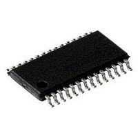
IC, DUAL SYNC BUCK CONVERTER, 28-TSSOP
Manufacturer
National Semiconductor
Datasheet
1.LM5642MTCNOPB.pdf
(28 pages)
Specifications of LM5642MTC
Primary Input Voltage
36V
No. Of Outputs
2
Output Voltage
32.4V
Output Current
20A
No. Of Pins
28
Operating Temperature Range
-40°C To +125°C
Power Dissipation Pd
1.1W
Lead Free Status / RoHS Status
Contains lead / RoHS non-compliant
Available stocks
Company
Part Number
Manufacturer
Quantity
Price

Part Number:
LM5642MTC
Manufacturer:
NS/国半
Quantity:
20 000
Part Number:
LM5642MTC/LM5642XMT
Manufacturer:
NS/国半
Quantity:
20 000
Company:
Part Number:
LM5642MTC/NOPB
Manufacturer:
NS
Quantity:
217
Part Number:
LM5642MTCX
Manufacturer:
NS/国半
Quantity:
20 000
Company:
Part Number:
LM5642MTCX/NOPB
Manufacturer:
TI
Quantity:
7 966


www.national.com
Connection Diagrams
Ordering Information
Pin Descriptions
KS1 (Pin 1): The positive (+) Kelvin sense for the internal
current sense amplifier of Channel 1. Use a separate trace to
connect this pin to the current-sense point. It should be con-
nected to VIN as close as possible to the current-sense
resistor. When no current-sense resistor is used, connect as
close as possible to the drain node of the upper MOSFET.
ILIM1 (Pin 2): Current limit threshold setting for Channel 1. It
sinks a constant current of 9.9 µA, which is converted to a
voltage across a resistor connected from this pin to VIN. The
voltage across the resistor is compared with either the V
the top MOSFET or the voltage across the external current
sense resistor to determine if an over-current condition has
occurred in Channel 1.
COMP1 (Pin 3): Compensation pin for Channel 1. This is the
output of the internal transconductance error amplifier. The
loop compensation network should be connected between
this pin and the signal ground, SGND (Pin 8).
FB1 (Pin 4): Feedback input for channel 1. Connect to VOUT
through a voltage divider to set the Channel 1 output voltage.
SYNC (Pin 5): The switching frequency of the LM5642 can
be synchronized to an external clock.
Order Number
LM5642MTCX
LM5642XMTX
LM5642MHX
LM5642MTC
LM5642XMT
LM5642MH
28-Lead eTSSOP
Top View
28-Lead TSSOP
Package Type
NSC Package Drawing
DS
20060102
of
MXA28A
MTC28
2
SYNC = LOW: Free running at 200 kHz for LM5642, and
at 375kHz for LM5642X. Channels are 180° out of phase.
SYNC = HIGH: Waiting for external clock
SYNC = Falling Edge: Channel 1 HDRV pin goes high.
Channel 2 HDRV pin goes high after 2.5 µs delay. The max-
imum SYNC pulse width must be greater than 100 ns.
For SYNC = Low operation, connect this pin to signal ground
through a 220 kΩ resistor.
UV_DELAY (Pin 6): A capacitor from this pin to ground sets
the delay time for UVP. The capacitor is charged from a 5 µA
current source. When UV_DELAY charges to 2.3V (typical),
the system immediately latches off. Connecting this pin to
ground will disable the output under-voltage protection.
VLIN5 (Pin 7): The output of an internal 5V LDO regulator
derived from VIN. It supplies the internal bias for the chip and
powers the bootstrap circuitry for gate drive. Bypass this pin
to signal ground with a minimum of 4.7 µF ceramic capacitor.
SGND (Pin 8): The ground connection for the signal-level cir-
cuitry. It should be connected to the ground rail of the system.
ON/SS1 (Pin 9): Channel 1 enable pin. This pin is internally
pulled up to one diode drop above VLIN5. Pulling this pin be-
low 1.2V (open-collector type) turns off Channel 1. If both ON/
SS1 and ON/SS2 pins are pulled below 1.2V, the whole chip
2500 Units on Tape and Reel
2500 Units on Tape and Reel
2500 Units on Tape and Reel
Top View
48 units per Rail
48 units per Rail
48 units per Rail
Supplied As
20060194
Related parts for LM5642MTC
Image
Part Number
Description
Manufacturer
Datasheet
Request
R

Part Number:
Description:
National Semiconductor [8-Bit D/A Converter]
Manufacturer:
National Semiconductor
Datasheet:
Part Number:
Description:
National Semiconductor [Media Coprocessor]
Manufacturer:
National Semiconductor
Datasheet:
Part Number:
Description:
Digitally Controlled Tone and Volume Circuit with Stereo Audio Power Amplifier, Microphone Preamp Stage and National 3D Sound
Manufacturer:
National Semiconductor
Datasheet:
Part Number:
Description:
Digitally Controlled Tone and Volume Circuit with Stereo Audio Power Amplifier, Microphone Preamp Stage and National 3D Sound
Manufacturer:
National Semiconductor
Datasheet:
Part Number:
Description:
AC97 Rev 2 Codec with Sample Rate Conversion and National 3D Sound
Manufacturer:
National Semiconductor
Part Number:
Description:
Manufacturer:
National Semiconductor
Datasheet:
Part Number:
Description:
Manufacturer:
National Semiconductor
Datasheet:
Part Number:
Description:
General Purpose, Low Voltage, Low Power, Rail-to-Rail Output Operational Amplifiers
Manufacturer:
National Semiconductor
Datasheet:
Part Number:
Description:
8-bit 20 MSPS flash A/D converter.
Manufacturer:
National Semiconductor
Datasheet:
Part Number:
Description:
Low Noise Quad Operational Amplifier
Manufacturer:
National Semiconductor
Datasheet:
Part Number:
Description:
Quad Differential Line Receivers
Manufacturer:
National Semiconductor
Datasheet:
Part Number:
Description:
Quad High Speed Trapezoidal? Bus Transceiver
Manufacturer:
National Semiconductor
Datasheet:
Part Number:
Description:
Dual Line Receiver
Manufacturer:
National Semiconductor
Datasheet:
Part Number:
Description:
TTL to 10k ECL Level Translator with Latch
Manufacturer:
National Semiconductor
Datasheet: