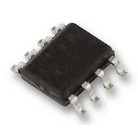
SI-8005Q Allegro Microsystems Inc, SI-8005Q Datasheet - Page 6

SI-8005Q
Manufacturer Part Number
SI-8005Q
Description
IC, BUCK, REG, 3.5A, 8HSOP
Manufacturer
Allegro Microsystems Inc
Datasheet
1.SI-8005Q.pdf
(12 pages)
Specifications of SI-8005Q
Primary Input Voltage
28V
No. Of Outputs
1
Output Voltage
24V
Output Current
3.5A
Voltage Regulator Case Style
HSOP
No. Of Pins
8
Operating Temperature Range
-30°C To +85°C
Base
RoHS Compliant
Package / Case
HSOP
Available stocks
Company
Part Number
Manufacturer
Quantity
Price
Company:
Part Number:
SI-8005Q
Manufacturer:
NEC
Quantity:
1 600
SI-8005Q
Component Selection for General Applications
Diode Di A Schottky-barrier diode must be used for Di. If other
diode types, such as fast recovery diodes, are used, the IC may
be destroyed because of reverse voltages applied by the recovery
voltage or turn-on voltage.
Choke Coil L1 If the winding resistance of the choke coil is too
high, IC efficiency may go down to the extent that the resistance
is beyond the rating. Because the overcurrent protection threshold
current is approximately 4 A, attention must be paid to the heat-
ing of the choke coil by magnetic saturation due to overload or
short-circulated load.
Capacitors C1, C2, and C5 Because large ripple currents for
SMPS flow across C1 and C2, capacitors with high frequency
and low impedance must be used. Especially when the impedance
of C2 is high, the switching waveform may not be normal at low
temperatures.
All external components should be mounted as closely as possible to the
SI-8005Q. The ground of all components should be connected at one point.
The exposed copper area on the PCB that is connected to the heat sink
on the reverse side of package is ground. Enlarging the PCB copper area
enhances thermal dissipation from the package.
Figure 1. Typical application circuit for general use
V
I I N
G N D
C1
EN
Vsw
Vin
C1
SS
COMP
C5
C5
C3
Recommended PCB Layout
O P EN
U1
C6
R3
7
8
C6
C4
S S
EN
D1
2
FB
I I N
C O M P
R2
S I - 8005Q
6
R3
C3
R1
Step-Down Switching Regulator with Current-Mode Control
1
B S
G N D
S W
FB
4
3
5
C4
L1
Application Information
115 Northeast Cutoff, Box 15036
Allegro MicroSystems, Inc.
Worcester, Massachusetts 01615-0036 (508) 853-5000
www.allegromicro.com
GND
C2
Di
V
R1
R2
L1
FB
Typical Application Diagram
Vout
I
A D J
G N D
C2
V
5 V
O
C5 is used to enable soft start. If the soft start function is not
used, leave the SS terminal open.
Resistors R1 and R2 R1 and R2 set the output voltage, V
Select the resistor values to set I
calculated by the following expression:
For optimum performance, minimize the distance between com-
ponents.
Phase Compensation Components C3, C6, and R3 The
stability and response of the loop is controlled through the COMP
pin. The COMP pin is the output of the internal transconductance
R
1
Component
C1 (2 ea)
C2 (2 ea)
C4, C5
V
C3
R1
R2
R3
L1
Di
O
U ni t : m m
I
ADJ
V
FB
Recommended Solder Pad Layout
10 μF / 50 V
22 μF / 16 V
220 pF
10 nF
10 μH
46 kΩ
5.1 kΩ
62 kΩ
0
V
1 .
O
Rating
10
0
5 .
3
2.80
,
4.30
ADJ
R
Murata, P/N GRM55DB31H106KA87
Murata, P/N GRM32ER71A226KE20
Murata, P/N GRM18 series
Murata, P/N GRM18 series
Sanken, P/N SPB-G56S or SJPB-L4
2
to 0.1 mA. R
I
V
ADJ
FB
Manufacturer
0
1 .
1.35
0
1
5 .
10
and R
3
≒
2
5
are
k
O
.
6


