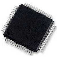
LPC2119FBD64 NXP Semiconductors, LPC2119FBD64 Datasheet - Page 7

LPC2119FBD64
Manufacturer Part Number
LPC2119FBD64
Description
16/32BIT MCU ARM7, 128K FLASH, 64LQFP
Manufacturer
NXP Semiconductors
Datasheet
1.LPC2119FBD64.pdf
(44 pages)
Specifications of LPC2119FBD64
No. Of I/o's
46
Ram Memory Size
16KB
Cpu Speed
60MHz
No. Of Timers
2
No. Of Pwm Channels
6
Digital Ic Case
RoHS Compliant
Core Size
32bit
Program Memory Size
128KB
Oscillator Type
External Only
Controller Family/series
LPC21xx
Rohs Compliant
Yes
Data Bus Width
16 bit, 32 bit
Program Memory Type
Flash
Data Ram Size
16 KB
Interface Type
CAN, I2C, JTAG, SPI, SSP, UART
Maximum Clock Frequency
60 MHz
Number Of Programmable I/os
46
Number Of Timers
2
Maximum Operating Temperature
+ 85 C
Mounting Style
SMD/SMT
Package / Case
LQFP
Minimum Operating Temperature
- 40 C
On-chip Adc
10 bit, 4 Channel
Lead Free Status / Rohs Status
Details
Available stocks
Company
Part Number
Manufacturer
Quantity
Price
Company:
Part Number:
LPC2119FBD64
Manufacturer:
NXP
Quantity:
5 000
Company:
Part Number:
LPC2119FBD64
Manufacturer:
NXP
Quantity:
748
Part Number:
LPC2119FBD64
Manufacturer:
NXP/恩智浦
Quantity:
20 000
Company:
Part Number:
LPC2119FBD64,151
Manufacturer:
NXP Semiconductors
Quantity:
10 000
Company:
Part Number:
LPC2119FBD64/01
Manufacturer:
NXP
Quantity:
8 000
Company:
Part Number:
LPC2119FBD64/01,15
Manufacturer:
Maxim
Quantity:
93
Company:
Part Number:
LPC2119FBD64/01,15
Manufacturer:
NXP Semiconductors
Quantity:
10 000
NXP Semiconductors
Table 3.
Product data sheet
LPC2109_2119_2129_6
Symbol
P0[15]/RI1/EINT2
P0[16]/EINT0/
MAT0[2]/CAP0[2]
P0[17]/CAP1[2]/
SCK1/MAT1[2]
P0[18]/CAP1[3]/
MISO1/MAT1[3]
P0[19]/MAT1[2]/
MOSI1/CAP1[2]
P0[20]/MAT1[3]/
SSEL1/EINT3
P0[21]/PWM5/
CAP1[3]
P0[22]/CAP0[0]/
MAT0[0]
P0[23]/RD2
P0[24]/TD2
P0[25]/RD1
P0[27]/AIN0/
CAP0[1]/MAT0[1]
P0[28]/AIN1/
CAP0[2]/MAT0[2]
P0[29]/AIN2/
CAP0[3]/MAT0[3]
P0[30]/AIN3/
EINT3/CAP0[0]
P1[0] to P1[31]
Pin description
Pin
45
46
47
53
54
55
1
2
3
5
9
11
13
14
15
…continued
Type Description
I
I
I
O
I
I
I/O
O
I
I/O
O
O
I/O
I
O
I
I
O
I
I
O
I
O
I
I
I
O
I
I
O
I
I
O
I
I
I
I/O
RI1 — Ring Indicator input for UART1.
EINT2 — External interrupt 2 input.
EINT0 — External interrupt 0 input.
MAT0[2] — Match output for Timer 0, channel 2.
CAP0[2] — Capture input for Timer 0, channel 2.
CAP1[2] — Capture input for Timer 1, channel 2.
SCK1 — Serial Clock for SPI1/SSP
slave.
MAT1[2] — Match output for Timer 1, channel 2.
CAP1[3] — Capture input for Timer 1, channel 3.
MISO1 — Master In Slave Out for SPI1/SSP
output from SPI slave.
MAT1[3] — Match output for Timer 1, channel 3.
MAT1[2] — Match output for Timer 1, channel 2.
MOSI1 — Master Out Slave In for SPI1/SSP
input to SPI slave.
CAP1[2] — Capture input for Timer 1, channel 2.
MAT1[3] — Match output for Timer 1, channel 3.
SSEL1 — Slave Select for SPI1/SSP
EINT3 — External interrupt 3 input.
PWM5 — Pulse Width Modulator output 5.
CAP1[3] — Capture input for Timer 1, channel 3.
CAP0[0] — Capture input for Timer 0, channel 0.
MAT0[0] — Match output for Timer 0, channel 0.
CAN2 receiver input (not available on LPC2109).
CAN2 transmitter output (not available on LPC2109).
CAN1 receiver input.
AIN0 — A/D converter, input 0. This analog input is always connected to its pin.
CAP0[1] — Capture input for Timer 0, channel 1.
MAT0[1] — Match output for Timer 0, channel 1.
AIN1 — A/D converter, input 1. This analog input is always connected to its pin.
CAP0[2] — Capture input for Timer 0, channel 2.
MAT0[2] — Match output for Timer 0, channel 2.
AIN2 — A/D converter, input 2. This analog input is always connected to its pin.
CAP0[3] — Capture input for Timer 0, Channel 3.
MAT0[3] — Match output for Timer 0, channel 3.
AIN3 — A/D converter, input 3. This analog input is always connected to its pin.
EINT3 — External interrupt 3 input.
CAP0[0] — Capture input for Timer 0, channel 0.
Port 1 is a 32-bit bidirectional I/O port with individual direction controls for each bit.
The operation of port 1 pins depends upon the pin function selected via the Pin
Connect Block. Pins 0 through 15 of port 1 are not available.
Rev. 06 — 10 December 2007
[1]
[1]
. SPI clock output from master or input to
LPC2109/2119/2129
. Selects the SPI interface as a slave.
Single-chip 16/32-bit microcontrollers
[1]
[1]
. Data output from SPI master or data
. Data input to SPI master or data
© NXP B.V. 2007. All rights reserved.
7 of 44


