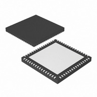
PIC24FJ256GA106-I/MR Microchip Technology, PIC24FJ256GA106-I/MR Datasheet - Page 30

PIC24FJ256GA106-I/MR
Manufacturer Part Number
PIC24FJ256GA106-I/MR
Description
IC, 16BIT MCU, PIC24F, 32MHZ, QFN-64
Manufacturer
Microchip Technology
Series
PIC® 24Fr
Datasheets
1.PIC24FJ128GA008-IPT.pdf
(12 pages)
2.PIC24FJ128GA106-IPT.pdf
(14 pages)
3.PIC24FJ128GA106-IPT.pdf
(330 pages)
4.PIC24FJ128GA106-IPT.pdf
(52 pages)
5.PIC24FJ256GA106-IPT.pdf
(59 pages)
6.PIC24FJ128GB110-IPF.pdf
(292 pages)
Specifications of PIC24FJ256GA106-I/MR
Controller Family/series
PIC24
No. Of I/o's
53
Ram Memory Size
16KB
Cpu Speed
32MHz
No. Of Timers
5
Core Size
16 Bit
Program Memory Size
256KB
Peripherals
ADC, Comparator, PWM, RTC, Timer
Core Processor
PIC
Speed
32MHz
Connectivity
I²C, PMP, SPI, UART/USART
Number Of I /o
53
Program Memory Type
FLASH
Ram Size
16K x 8
Voltage - Supply (vcc/vdd)
2 V ~ 3.6 V
Data Converters
A/D 16x10b
Oscillator Type
Internal
Operating Temperature
-40°C ~ 85°C
Package / Case
64-VFQFN, Exposed Pad
Processor Series
PIC24FJ
Core
PIC
Data Bus Width
16 bit
Data Ram Size
16 KB
Interface Type
I2C, SPI, UART
Maximum Clock Frequency
32 MHz
Number Of Programmable I/os
52
Number Of Timers
5
Maximum Operating Temperature
+ 85 C
Mounting Style
SMD/SMT
3rd Party Development Tools
52713-733, 52714-737, 53276-922, EWDSPIC
Development Tools By Supplier
PG164130, DV164035, DV244005, DV164005, PG164120, DM240001, DM240011
Minimum Operating Temperature
- 40 C
On-chip Adc
10 bit, 16 Channel
Lead Free Status / RoHS Status
Lead free / RoHS Compliant
For Use With
876-1004 - PIC24 BREAKOUT BOARD
Eeprom Size
-
Lead Free Status / Rohs Status
Details
PIC24FJXXXDA1/DA2/GB2/GA3
FIGURE 4-2:
FIGURE 4-3:
DS39970B-page 30
MCLR
V
PGEDx
PGECx
Enter ICSP™ Mode
Resident in Memory
DD
Prog. Executive is
Application ID
Application ID
from Address
Read the
8007F0h
CCh?
Start
End
Is
Yes
P6
CONFIRMING PRESENCE
OF PROGRAMMING
EXECUTIVE
ENTERING ENHANCED ICSP™ MODE
No
Prog. Executive must
be Programmed
P14
P18
V
b31
IH
0
b30
1
Program/Verify Entry Code = 4D434850h
b29
0
P1A
b28
0
P1B
b27
1
Program/Verify mode requires three steps:
4.3
As displayed in
1.
2.
3.
The programming voltage applied to MCLR is V
which
PIC24FJXXXDA1/DA2/GB2/GA3 devices. There is no
minimum time requirement for holding at V
is removed, an interval of at least P18 must elapse
before presenting the key sequence on PGEDx.
The key sequence is a specific 32-bit pattern:
‘0100 1101 0100 0011 0100 1000 0101 0000’
(more easily remembered as 4D434850h in hexa-
decimal format). The device will enter Program/Verify
mode only if the key sequence is valid. The MSb of the
most significant nibble must be shifted in first.
Once the key sequence is complete, V
applied to MCLR and held at that level for as long as
Program/Verify mode is to be maintained. An interval of
at least time, P19 and P7, must elapse before present-
ing data on PGEDx. Signals appearing on PGEDx,
before P7 has elapsed, will not be interpreted as valid.
On successful entry, the program memory can be
accessed and programmed in serial fashion. While in
the Program/Verify mode, all unused I/Os are placed in
the high-impedance state.
...
The MCLR pin is briefly driven high, then low.
A 32-bit key sequence is clocked into PGEDx.
MCLR is then driven high within a specified
period and held.
is
Entering Enhanced ICSP Mode
b3
0
essentially
b2
0
Figure
b1
0
V
4-3, entering Enhanced ICSP
2010 Microchip Technology Inc.
IH
V
b0
0
DD
P19
in
the
P7
IH
IH
. After V
case
must be
IH
of
IH
,


