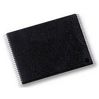
M29F200BB70N6E STMicroelectronics, M29F200BB70N6E Datasheet - Page 6

M29F200BB70N6E
Manufacturer Part Number
M29F200BB70N6E
Description
IC, FLASH, 2MBIT, 70NS, TSOP-48
Manufacturer
STMicroelectronics
Datasheet
1.M29F200BB70N6E.pdf
(23 pages)
Specifications of M29F200BB70N6E
Memory Type
Flash - Boot Block
Memory Size
2Mbit
Memory Configuration
256K X 8 / 128K X 16
Access Time
70ns
Supply Voltage Range
4.5V To 5.5V
Memory Case Style
TSOP
No. Of Pins
48
Lead Free Status / RoHS Status
Lead free / RoHS Compliant
M29F200BT, M29F200BB
Standby. When Chip Enable is High, V
Data Inputs/Outputs pins are placed in the high-
impedance state and the Supply Current is re-
duced to the Standby level.
When Chip Enable is at V
reduced to the TTL Standby Supply Current, I
To further reduce the Supply Current to the CMOS
Standby Supply Current, I
be held within V
levels see Table 13, DC Characteristics.
During program or erase operations the memory
will continue to use the Program/Erase Supply
Current, I
til the operation completes.
Automatic Standby. If CMOS levels (V
are used to drive the bus and the bus is inactive for
150ns or more the memory enters Automatic
Standby where the internal Supply Current is re-
duced to the CMOS Standby Supply Current, I
The Data Inputs/Outputs will still output data if a
Bus Read operation is in progress.
Special Bus Operations
Additional bus operations can be performed to
read the Electronic Signature and also to apply
and remove Block Protection. These bus opera-
tions are intended for use by programming equip-
ment and are not usually used in applications.
They require V
Electronic Signature. The memory has two
codes, the manufacturer code and the device
code, that can be read to identify the memory.
These codes can be read by applying the signals
listed in Tables 5 and 6, Bus Operations.
Block Protection and Blocks Unprotection. Each
block can be separately protected against acci-
dental Program or Erase. Protected blocks can be
unprotected to allow data to be changed.
There are two methods available for protecting
and unprotecting the blocks, one for use on pro-
gramming equipment and the other for in-system
use. For further information refer to Application
Note AN1122, Applying Protection and Unprotec-
tion to M29 Series Flash.
6/22
CC4
, for Program or Erase operations un-
ID
CC
to be applied to some pins.
± 0.2V. For Standby current
CC3
IH
the Supply Current is
, Chip Enable should
CC
± 0.2V)
IH
, the
CC2
CC3
.
.
COMMAND INTERFACE
All Bus Write operations to the memory are inter-
preted by the Command Interface. Commands
consist of one or more sequential Bus Write oper-
ations. Failure to observe a valid sequence of Bus
Write operations will result in the memory return-
ing to Read mode. The long command sequences
are imposed to maximize data security.
The address used for the commands changes de-
pending on whether the memory is in 16-bit or 8-
bit mode. See either Table 7, or 8, depending on
the configuration that is being used, for a summary
of the commands.
Read/Reset Command. The Read/Reset com-
mand returns the memory to its Read mode where
it behaves like a ROM or EPROM. It also resets
the errors in the Status Register. Either one or
three Bus Write operations can be used to issue
the Read/Reset command.
If the Read/Reset command is issued during a
Block Erase operation or following a Programming
or Erase error then the memory will take upto 10
to abort. During the abort period no valid data can
be read from the memory. Issuing a Read/Reset
command during a Block Erase operation will
leave invalid data in the memory.
Auto Select Command. The Auto Select com-
mand is used to read the Manufacturer Code, the
Device Code and the Block Protection Status.
Three consecutive Bus Write operations are re-
quired to issue the Auto Select command. Once
the Auto Select command is issued the memory
remains in Auto Select mode until another com-
mand is issued.
From the Auto Select mode the Manufacturer
Code can be read using a Bus Read operation
with A0 = V
may be set to either V
Code for STMicroelectronics is 0020h.
The Device Code can be read using a Bus Read
operation with A0 = V
address bits may be set to either V
Device Code for the M29F200BT is 00D3h and for
the M29F200BB is 00D4h.
IL
and A1 = V
IL
IH
or V
IL
and A1 = V
. The other address bits
IH
. The Manufacturer
IL
IL
or V
. The other
IH
. The
µs


