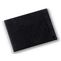
M29F200BB70N6E STMicroelectronics, M29F200BB70N6E Datasheet - Page 3

M29F200BB70N6E
Manufacturer Part Number
M29F200BB70N6E
Description
IC, FLASH, 2MBIT, 70NS, TSOP-48
Manufacturer
STMicroelectronics
Datasheet
1.M29F200BB70N6E.pdf
(23 pages)
Specifications of M29F200BB70N6E
Memory Type
Flash - Boot Block
Memory Size
2Mbit
Memory Configuration
256K X 8 / 128K X 16
Access Time
70ns
Supply Voltage Range
4.5V To 5.5V
Memory Case Style
TSOP
No. Of Pins
48
Lead Free Status / RoHS Status
Lead free / RoHS Compliant
Table 2. Absolute Maximum Ratings
Note: 1. Except for the rating "Operating Temperature Range", stresses above those listed in the Table "Absolute Maximum Ratings" may
The blocks in the memory are asymmetrically ar-
ranged, see Tables 3 and 4, Block Addresses. The
first or last 64 Kbytes have been divided into four
additional blocks. The 16 Kbyte Boot Block can be
used for small initialization code to start the micro-
processor, the two 8 Kbyte Parameter Blocks can
be used for parameter storage and the remaining
32K is a small Main Block where the application
may be stored.
Table 3. Top Boot Block Addresses,
M29F200BT
#
6
5
4
3
2
1
0
Symbol
(Kbytes)
2. Minimum Voltage may undershoot to –2V during transition and for less than 20ns during transitions.
V
T
T
V
IO
V
BIAS
Size
T
STG
cause permanent damage to the device. These are stress ratings only and operation of the device at these or any other conditions
above those indicated in the Operating sections of this specification is not implied. Exposure to Absolute Maximum Rating condi-
tions for extended periods may affect device reliability. Refer also to the STMicroelectronics SURE Program and other relevant qual-
ity documents.
CC
16
32
64
64
64
ID
A
8
8
(2)
3C000h-3FFFFh
3A000h-3BFFFh
Address Range
38000h-39FFFh
30000h-37FFFh
20000h-2FFFFh
10000h-1FFFFh
00000h-0FFFFh
Ambient Operating Temperature (Temperature Range Option 1)
Ambient Operating Temperature (Temperature Range Option 6)
Ambient Operating Temperature (Temperature Range Option 3)
Temperature Under Bias
Storage Temperature
Input or Output Voltage
Supply Voltage
Identification Voltage
(x8)
1D000h-1DFFFh
1C000h-1CFFFh
Address Range
1E000h-1FFFFh
18000h-1BFFFh
08000h-0FFFFh
10000h-17FFFh
00000h-07FFFh
(x16)
(1)
Parameter
Chip Enable, Output Enable and Write Enable sig-
nals control the bus operation of the memory.
They allow simple connection to most micropro-
cessors, often without additional logic.
The memory is offered in TSOP48 (12 x 20mm)
and SO44 packages and it is supplied with all the
bits erased (set to ’1’).
Table 4. Bottom Boot Block Addresses,
M29F200BB
#
6
5
4
3
2
1
0
(Kbytes)
Size
64
64
64
32
16
8
8
Address Range
30000h-3FFFFh
20000h-2FFFFh
10000h-1FFFFh
08000h-0FFFFh
06000h-07FFFh
04000h-05FFFh
00000h-03FFFh
M29F200BT, M29F200BB
(x8)
–0.6 to 13.5
–40 to 125
–50 to 125
–65 to 150
–40 to 85
–0.6 to 6
–0.6 to 6
0 to 70
Value
Address Range
18000h-1FFFFh
08000h-0FFFFh
10000h-17FFFh
04000h-07FFFh
03000h-03FFFh
02000h-02FFFh
00000h-01FFFh
(x16)
Unit
°C
°C
°C
°C
°C
V
V
V
3/22


