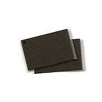
S29JL064H70TFI000 Spansion Inc., S29JL064H70TFI000 Datasheet - Page 42

S29JL064H70TFI000
Manufacturer Part Number
S29JL064H70TFI000
Description
IC, FLASH, 64MBIT, 70NS, TSOP-48
Manufacturer
Spansion Inc.
Datasheet
1.S29JL064H90TFI000.pdf
(61 pages)
Specifications of S29JL064H70TFI000
Memory Type
Flash
Memory Size
64Mbit
Memory Configuration
8M X 8 / 4M X 16
Ic Interface Type
CFI, Parallel
Access Time
70ns
Supply Voltage Range
2.7 To 3.6 V
Memory Case Style
TSOP
Data Bus Width
8 bit, 16 bit
Architecture
Boot Sector
Interface Type
Conventional
Supply Voltage (max)
3.6 V
Supply Voltage (min)
2.7 V
Maximum Operating Current
10 mA
Mounting Style
SMD/SMT
Operating Temperature
+ 85 C
Package / Case
TSOP-48
Lead Free Status / RoHS Status
Lead free / RoHS Compliant
Lead Free Status / RoHS Status
Lead free / RoHS Compliant, Lead free / RoHS Compliant
Available stocks
Company
Part Number
Manufacturer
Quantity
Price
Part Number:
S29JL064H70TFI000
Manufacturer:
PANSION
Quantity:
20 000
Company:
Part Number:
S29JL064H70TFI000H
Manufacturer:
SPANSION
Quantity:
121
12. Absolute Maximum Ratings
42
Notes
1. DQ5 switches to 1 when an Embedded Program or Embedded Erase operation has exceeded the maximum timing limits. Refer to the
2. DQ7 and DQ2 require a valid address when reading status information. Refer to the appropriate subsection for further details.
3. When reading write operation status bits, the system must always provide the bank address where the Embedded Algorithm is in
Notes
1. Minimum DC voltage on input or I/O pins is –0.5 V. During voltage transitions, input or I/O pins may overshoot V
2. Minimum DC input voltage on pins A9, OE#, RESET#, and WP#/ACC is –0.5 V. During voltage transitions, A9, OE#, WP#/ACC, and
3. No more than one output may be shorted to ground at a time. Duration of the short circuit should not be greater than one second.
4. Stresses above those listed under “Absolute Maximum Ratings” may cause permanent damage to the device. This is a stress rating only;
Standard
Mode
Erase
Suspend
Mode
Storage Temperature, Plastic Packages
Ambient Temperature with Power Applied
Voltage with Respect to Ground
Output Short Circuit Current
section on DQ5 for more information.
progress. The device outputs array data if the system addresses a non-busy bank.
up to 20 ns. Maximum DC voltage on input or I/O pins is V
pins may overshoot to V
RESET# may overshoot V
+12.5 V which may overshoot to +14.0 V for periods up to 20 ns. Maximum DC input voltage on WP#/ACC is +9.5 V which may overshoot
to +12.0 V for periods up to 20 ns.
functional operation of the device at these or any other conditions above those indicated in the operational sections of this data sheet is
not implied. Exposure of the device to absolute maximum rating conditions for extended periods may affect device reliability.
V
A9, OE#, and RESET#
WP#/ACC
All other pins (Note 1)
CC
(Note 1)
Embedded Program Algorithm
Embedded Erase Algorithm
Erase-Suspend-Read
Erase-Suspend-Program
CC
(Note 2)
Status
(Note 3)
SS
+2.0 V for periods up to 20 ns. See
to –2.0 V for periods of up to 20 ns. See
Figure 12.1 Maximum Negative Overshoot Waveform
Figure 12.2 Maximum Positive Overshoot Waveform
Erase
Suspended Sector
Non-Erase Suspended
Sector
+2.0 V
+0.5 V
+0.8 V
–0.5 V
–2.0 V
2.0 V
V
V
CC
CC
Table 11.1 Write Operation Status
S29JL064H
D a t a
20 ns
20 ns
CC
+0.5 V. See
(Note 2)
Figure 12.2 on page
DQ7#
DQ7#
Data
DQ7
0
1
S h e e t
20 ns
20 ns
Figure 12.1 on page
Figure 12.1 on page
No toggle
Toggle
Toggle
Toggle
20 ns
20 ns
DQ6
Data
42.
S29JL064H_00_A8 September 8, 2009
(Note 1)
DQ5
Data
42. Maximum DC input voltage on pin A9 is
0
0
0
0
42. During voltage transitions, input or I/O
DQ3
Data
N/A
N/A
N/A
1
–0.5 V to V
–0.5 V to +12.5 V
–0.5 V to +10.5 V
–65°C to +150°C
–65°C to +125°C
–0.5 V to +4.0 V
SS
200 mA
No toggle
(Note 2)
to –2.0 V for periods of
Toggle
Toggle
DQ2
Data
N/A
CC
+0.5 V
RY/BY#
0
0
1
1
0


