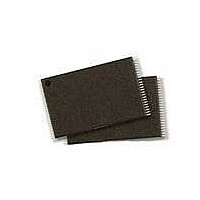
S29JL064H70TFI000 Spansion Inc., S29JL064H70TFI000 Datasheet - Page 16

S29JL064H70TFI000
Manufacturer Part Number
S29JL064H70TFI000
Description
IC, FLASH, 64MBIT, 70NS, TSOP-48
Manufacturer
Spansion Inc.
Datasheet
1.S29JL064H90TFI000.pdf
(61 pages)
Specifications of S29JL064H70TFI000
Memory Type
Flash
Memory Size
64Mbit
Memory Configuration
8M X 8 / 4M X 16
Ic Interface Type
CFI, Parallel
Access Time
70ns
Supply Voltage Range
2.7 To 3.6 V
Memory Case Style
TSOP
Data Bus Width
8 bit, 16 bit
Architecture
Boot Sector
Interface Type
Conventional
Supply Voltage (max)
3.6 V
Supply Voltage (min)
2.7 V
Maximum Operating Current
10 mA
Mounting Style
SMD/SMT
Operating Temperature
+ 85 C
Package / Case
TSOP-48
Lead Free Status / RoHS Status
Lead free / RoHS Compliant
Lead Free Status / RoHS Status
Lead free / RoHS Compliant, Lead free / RoHS Compliant
Available stocks
Company
Part Number
Manufacturer
Quantity
Price
Part Number:
S29JL064H70TFI000
Manufacturer:
PANSION
Quantity:
20 000
Company:
Part Number:
S29JL064H70TFI000H
Manufacturer:
SPANSION
Quantity:
121
8.4
8.5
8.6
8.7
16
Simultaneous Read/Write Operations with Zero Latency
Standby Mode
Automatic Sleep Mode
RESET#: Hardware Reset Pin
This device is capable of reading data from one bank of memory while programming or erasing in the other
bank of memory. An erase operation may also be suspended to read from or program to another location
within the same bank (except the sector being erased).
cycles may be initiated for simultaneous operation with zero latency. I
on page 43
When the system is not reading or writing to the device, it can place the device in the standby mode. In this
mode, current consumption is greatly reduced, and the outputs are placed in the high impedance state,
independent of the OE# input.
The device enters the CMOS standby mode when the CE# and RESET# pins are both held at V
(Note that this is a more restricted voltage range than V
V
requires standard access time (t
before it is ready to read data.
If the device is deselected during erasure or programming, the device draws active current until the operation
is completed.
I
The automatic sleep mode minimizes Flash device energy consumption. The device automatically enables
this mode when addresses remain stable for t
CE#, WE#, and OE# control signals. Standard address access timings provide new data when addresses are
changed. While in sleep mode, output data is latched and always available to the system. I
Characteristics on page 43
The RESET# pin provides a hardware method of resetting the device to reading array data. When the
RESET# pin is driven low for at least a period of t
progress, tristates all output pins, and ignores all read/write commands for the duration of the RESET# pulse.
The device also resets the internal state machine to reading array data. The operation that was interrupted
should be reinitiated once the device is ready to accept another command sequence, to ensure data integrity.
Current is reduced for the duration of the RESET# pulse. When RESET# is held at V
draws CMOS standby current (I
will be greater.
The RESET# pin may be tied to the system reset circuitry. A system reset would thus also reset the Flash
memory, enabling the system to read the boot-up firmware from the Flash memory.
If RESET# is asserted during a program or erase operation, the RY/BY# pin remains a “0” (busy) until the
internal reset operation is complete, which requires a time of t
system can thus monitor RY/BY# to determine whether the reset operation is complete. If RESET# is
asserted when a program or erase operation is not executing (RY/BY# pin is “1”), the reset operation is
completed within a time of t
RESET# pin returns to V
Refer to
diagram.
CC3
CC
± 0.3 V, the device will be in the standby mode, but the standby current will be greater. The device
in
DC Characteristics on page 43
AC Characteristics on page 46
represent the current specifications for read-while-program and read-while-erase, respectively.
IH
.
READY
represents the automatic sleep mode current specification.
CC4
CE
(not during Embedded Algorithms). The system can read data t
) for read access when the device is in either of these standby modes,
). If RESET# is held at V
represents the standby current specification.
for RESET# parameters and to
S29JL064H
D a t a
ACC
RP
+ 30 ns. The automatic sleep mode is independent of the
, the device immediately terminates any operation in
S h e e t
IH
Figure 17.8 on page 51
.) If CE# and RESET# are held at V
IL
READY
but not within V
(during Embedded Algorithms). The
CC6
Figure 17.2 on page 47
S29JL064H_00_A8 September 8, 2009
and I
SS
CC7
shows how read and write
±0.3 V, the standby current
in the
SS
±0.3 V, the device
DC Characteristics
CC5
IH
, but not within
in
for the timing
CC
RH
DC
± 0.3 V.
after the


