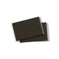
S29JL064H70TFI000 Spansion Inc., S29JL064H70TFI000 Datasheet - Page 33

S29JL064H70TFI000
Manufacturer Part Number
S29JL064H70TFI000
Description
IC, FLASH, 64MBIT, 70NS, TSOP-48
Manufacturer
Spansion Inc.
Datasheet
1.S29JL064H90TFI000.pdf
(61 pages)
Specifications of S29JL064H70TFI000
Memory Type
Flash
Memory Size
64Mbit
Memory Configuration
8M X 8 / 4M X 16
Ic Interface Type
CFI, Parallel
Access Time
70ns
Supply Voltage Range
2.7 To 3.6 V
Memory Case Style
TSOP
Data Bus Width
8 bit, 16 bit
Architecture
Boot Sector
Interface Type
Conventional
Supply Voltage (max)
3.6 V
Supply Voltage (min)
2.7 V
Maximum Operating Current
10 mA
Mounting Style
SMD/SMT
Operating Temperature
+ 85 C
Package / Case
TSOP-48
Lead Free Status / RoHS Status
Lead free / RoHS Compliant
Lead Free Status / RoHS Status
Lead free / RoHS Compliant, Lead free / RoHS Compliant
Available stocks
Company
Part Number
Manufacturer
Quantity
Price
Part Number:
S29JL064H70TFI000
Manufacturer:
PANSION
Quantity:
20 000
Company:
Part Number:
S29JL064H70TFI000H
Manufacturer:
SPANSION
Quantity:
121
September 8, 2009 S29JL064H_00_A8
10.5.1
Unlock Bypass Command Sequence
The unlock bypass feature allows the system to program bytes or words to a bank faster than using the
standard program command sequence. The unlock bypass command sequence is initiated by first writing two
unlock cycles. This is followed by a third write cycle containing the unlock bypass command, 20h. That bank
then enters the unlock bypass mode. A two-cycle unlock bypass program command sequence is all that is
required to program in this mode. The first cycle in this sequence contains the unlock bypass program
command, A0h; the second cycle contains the program address and data. Additional data is programmed in
the same manner. This mode dispenses with the initial two unlock cycles required in the standard program
command sequence, resulting in faster total programming time.
requirements for the command sequence.
During the unlock bypass mode, only the Unlock Bypass Program and Unlock Bypass Reset commands are
valid. To exit the unlock bypass mode, the system must issue the two-cycle unlock bypass reset command
sequence. (See
The device offers accelerated program operations through the WP#/ACC pin. When the system asserts V
on the WP#/ACC pin, the device automatically enters the Unlock Bypass mode. The system may then write
the two-cycle Unlock Bypass program command sequence. The device uses the higher voltage on the WP#/
ACC pin to accelerate the operation. Note that the WP#/ACC pin must not be at V
than accelerated programming, or device damage may result. In addition, the WP#/ACC pin must not be left
floating or unconnected; inconsistent behavior of the device may result.
Figure 10.1 on page 33
Operations on page 49
Note
1. See
Table 10.1 on page 36
Table 10.1 on page
for parameters, and
illustrates the algorithm for the program operation. Refer to
for program command sequence.
D a t a
Increment Address
S h e e t
36).
Figure 10.1 Program Operation
S29JL064H
Embedded
in progress
algorithm
Program
Figure 17.5 on page 50
No
Command Sequence
Write Program
Last Address?
Programming
from System
Verify Data?
Completed
Data Poll
START
Table 10.1 on page 36
Yes
Yes
for timing diagrams.
No
HH
Erase and Program
for any operation other
shows the
HH
33


