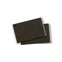
S29JL032H90TFI320 Spansion Inc., S29JL032H90TFI320 Datasheet - Page 38

S29JL032H90TFI320
Manufacturer Part Number
S29JL032H90TFI320
Description
IC, FLASH, 32MBIT, 90NS, TSOP-48
Manufacturer
Spansion Inc.
Datasheet
1.S29JL032H90TFI320.pdf
(61 pages)
Specifications of S29JL032H90TFI320
Memory Type
Flash
Memory Size
32Mbit
Memory Configuration
4M X 8 / 2M X 16
Ic Interface Type
CFI, Parallel
Access Time
90ns
Supply Voltage Range
2.7 To 3.6 V
Memory Case Style
TSOP
Data Bus Width
8 bit, 16 bit
Architecture
Boot Sector
Interface Type
Conventional
Supply Voltage (max)
3.6 V
Supply Voltage (min)
2.7 V
Maximum Operating Current
2 mA
Mounting Style
SMD/SMT
Operating Temperature
+ 85 C
Package / Case
TSOP-48
Rohs Compliant
YES
No. Of Pins
48
Lead Free Status / RoHS Status
Lead free / RoHS Compliant
Lead Free Status / RoHS Status
Lead free / RoHS Compliant, Lead free / RoHS Compliant
Available stocks
Company
Part Number
Manufacturer
Quantity
Price
Company:
Part Number:
S29JL032H90TFI320
Manufacturer:
Spansion
Quantity:
135
Company:
Part Number:
S29JL032H90TFI320
Manufacturer:
PANASONIC
Quantity:
4 314
Part Number:
S29JL032H90TFI320
Manufacturer:
SPANSION
Quantity:
20 000
10. The data is 42h for customer locked, and 82h for not customer locked. Some current and most future Spansion devices (including future revisions of this device)
11. The data is 00h for an unprotected sector/sector block and 01h for a protected sector/sector block.
12. The Unlock Bypass command is required prior to the Unlock Bypass Program command.
13. The Unlock Bypass Reset command is required to return to the read mode when the bank is in the unlock bypass mode.
14. The system may read and program in non-erasing sectors, or enter the autoselect mode, when in the Erase Suspend mode. The Erase Suspend command is
15. The Erase Resume command is valid only during the Erase Suspend mode, and requires the bank address.
16. Command is valid when device is ready to read array data or when device is in autoselect mode.
11. Write Operation Status
11.1
38
will offer an option for programming and permanently locking the Secured Silicon Sector at the factory. The Secured Silicon Indicator data will change to 82h for
factory locked, 42h for customer locked, and 02h (no longer 82h) for not factory/customer locked.
valid only during a sector erase operation, and requires the bank address.
DQ7: Data# Polling
The device provides several bits to determine the status of a program or erase operation: DQ2, DQ3, DQ5,
DQ6, and DQ7.
and DQ6 each offer a method for determining whether a program or erase operation is complete or in
progress. The device also provides a hardware-based output signal, RY/BY#, to determine whether an
Embedded Program or Erase operation is in progress or has been completed.
The Data# Polling bit, DQ7, indicates to the host system whether an Embedded Program or Erase algorithm
is in progress or completed, or whether a bank is in Erase Suspend. Data# Polling is valid after the rising
edge of the final WE# pulse in the command sequence.
During the Embedded Program algorithm, the device outputs on DQ7 the complement of the datum
programmed to DQ7. This DQ7 status also applies to programming during Erase Suspend. When the
Embedded Program algorithm is complete, the device outputs the datum programmed to DQ7. The system
must provide the program address to read valid status information on DQ7. If a program address falls within a
protected sector, Data# Polling on DQ7 is active for approximately 1 µs, then that bank returns to the read
mode.
During the Embedded Erase algorithm, Data# Polling produces a “0” on DQ7. When the Embedded Erase
algorithm is complete, or if the bank enters the Erase Suspend mode, Data# Polling produces a “1” on DQ7.
The system must provide an address within any of the sectors selected for erasure to read valid status
information on DQ7.
After an erase command sequence is written, if all sectors selected for erasing are protected, Data# Polling
on DQ7 is active for approximately 100 µs, then the bank returns to the read mode. If not all selected sectors
are protected, the Embedded Erase algorithm erases the unprotected sectors, and ignores the selected
sectors that are protected. However, if the system reads DQ7 at an address within a protected sector, the
status may not be valid.
When the system detects DQ7 has changed from the complement to true data, it can read valid data at
DQ15–DQ0 (or DQ7–DQ0 for x8-only device) on the following read cycles. Just prior to the completion of an
Embedded Program or Erase operation, DQ7 may change asynchronously with DQ15–DQ8 (DQ7–DQ0 for
x8-only device) while Output Enable (OE#) is asserted low. That is, the device may change from providing
status information to valid data on DQ7. Depending on when the system samples the DQ7 output, it may read
the status or valid data. Even if the device has completed the program or erase operation and DQ7 has valid
data, the data outputs on DQ15–DQ0 may be still invalid. Valid data on DQ15–DQ0 (or DQ7–DQ0 for x8-only
device) will appear on successive read cycles.
Table 11.1 on page 42
Polling algorithm.
Table 11.1 on page 42
Figure 17.9 on page 53
shows the outputs for Data# Polling on DQ7.
and the following subsections describe the function of these bits. DQ7
S29JL032H
shows the Data# Polling timing diagram.
D a t a
S h e e t
Figure 11.1 on page 39
S29JL032H_00_B8 August 31, 2009
shows the Data#


