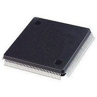
EPM7160SQC160-10N Altera, EPM7160SQC160-10N Datasheet - Page 22

EPM7160SQC160-10N
Manufacturer Part Number
EPM7160SQC160-10N
Description
IC PLD EEPROM 160 MACROCELL 10NS QFP-160
Manufacturer
Altera
Series
MAX 7000Sr
Datasheet
1.EPM7064STC44-10.pdf
(66 pages)
Specifications of EPM7160SQC160-10N
Cpld Type
EEPROM
No. Of Macrocells
160
No. Of I/o's
104
Propagation Delay
10ns
Global Clock Setup Time
3.4ns
Frequency
149.3MHz
Supply Voltage Range
4.75V To 5.25V
Family Name
MAX 7000S
Memory Type
EEPROM
# Macrocells
160
Number Of Usable Gates
3200
Frequency (max)
125MHz
Propagation Delay Time
10ns
Number Of Logic Blocks/elements
10
# I/os (max)
104
Operating Supply Voltage (typ)
5V
In System Programmable
Yes
Operating Supply Voltage (min)
4.75V
Operating Supply Voltage (max)
5.25V
Operating Temp Range
0C to 70C
Operating Temperature Classification
Commercial
Mounting
Surface Mount
Pin Count
160
Package Type
PQFP
Lead Free Status / RoHS Status
Lead free / RoHS Compliant
Lead Free Status / RoHS Status
Lead free / RoHS Compliant
Available stocks
Company
Part Number
Manufacturer
Quantity
Price
MAX 7000 Programmable Logic Device Family Data Sheet
IEEE Std.
1149.1 (JTAG)
Boundary-Scan
Support
22
SAMPLE/PRELOAD
EXTEST
BYPASS
IDCODE
ISP Instructions
Table 9. MAX 7000 JTAG Instructions
JTAG Instruction
EPM7128S
EPM7160S
EPM7192S
EPM7256S
EPM7128S
EPM7160S
EPM7192S
EPM7256S
EPM7032S
EPM7064S
EPM7128S
EPM7160S
EPM7192S
EPM7256S
EPM7032S
EPM7064S
EPM7128S
EPM7160S
EPM7192S
EPM7256S
EPM7032S
EPM7064S
EPM7128S
EPM7160S
EPM7192S
EPM7256S
Devices
MAX 7000 devices support JTAG BST circuitry as specified by IEEE Std.
1149.1-1990.
MAX 7000 family. The pin-out tables (see the Altera web site
(http://www.altera.com) or the Altera Digital Library for pin-out
information) show the location of the JTAG control pins for each device.
If the JTAG interface is not required, the JTAG pins are available as user
I/O pins.
Allows a snapshot of signals at the device pins to be captured and
examined during normal device operation, and permits an initial data
pattern output at the device pins.
Allows the external circuitry and board-level interconnections to be
tested by forcing a test pattern at the output pins and capturing test
results at the input pins.
Places the 1-bit bypass register between the TDI and TDO pins, which
allows the BST data to pass synchronously through a selected device
to adjacent devices during normal device operation.
Selects the IDCODE register and places it between TDI and TDO,
allowing the IDCODE to be serially shifted out of TDO.
These instructions are used when programming MAX 7000S devices
via the JTAG ports with the MasterBlaster, ByteBlasterMV, BitBlaster
download cable, or using a Jam File (.jam), Jam Byte-Code file (.jbc),
or Serial Vector Format file (.svf) via an embedded processor or test
equipment.
Table 9
describes the JTAG instructions supported by the
Description
Altera Corporation


