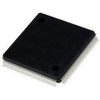
LFE2-12E-6QN208C LATTICE SEMICONDUCTOR, LFE2-12E-6QN208C Datasheet - Page 32

LFE2-12E-6QN208C
Manufacturer Part Number
LFE2-12E-6QN208C
Description
IC, LATTICEECP2 FPGA, 420MHZ, QFP-208
Manufacturer
LATTICE SEMICONDUCTOR
Series
LatticeECP2r
Datasheet
1.LFE2-12E-5FN256C.pdf
(385 pages)
Specifications of LFE2-12E-6QN208C
No. Of Logic Blocks
12000
No. Of Macrocells
6000
No. Of Speed Grades
6
No. Of I/o's
131
Clock Management
DLL, PLL
I/o Supply Voltage
3.465V
Total Ram Bits
221Kbit
Lead Free Status / RoHS Status
Lead free / RoHS Compliant
Available stocks
Company
Part Number
Manufacturer
Quantity
Price
Company:
Part Number:
LFE2-12E-6QN208C
Manufacturer:
Lattice Semiconductor Corporation
Quantity:
10 000
- Current page: 32 of 385
- Download datasheet (3Mb)
Lattice Semiconductor
Figure 2-28. PIC Diagram
Two adjacent PIOs can be joined to provide a differential I/O pair (labeled as “T” and “C”) as shown in Figure 2-28.
The PAD Labels “T” and “C” distinguish the two PIOs. Approximately 50% of the PIO pairs on the left and right
edges of the device can be configured as true LVDS outputs. All I/O pairs can operate as inputs.
DDRCLKPOL*
*Signals are available on left/right/bottom edges only.
** Selected blocks.
DQSXFER*
QNEG0*
QNEG1*
ONEG2*
QPOS0*
QPOS1*
OPOS2*
ONEG0
OPOS0
ONEG1
INDD
OPOS1
INCK**
ECLK1
ECLK2
IPOS0
IPOS1
GSRN
INFF
CLK
LSR
CE
TD
Control
Muxes
CLK1
CLK0
CEO
GSR
LSR
CEI
2-29
PIOA
Register
Register
Register
Tristate
Output
Block
Block
Block
Input
PIOB
IOLD0
IOLT0
DI
LatticeECP2/M Family Data Sheet
Buffer
sysIO
PADB
PADA
“C”
“T”
Architecture
Related parts for LFE2-12E-6QN208C
Image
Part Number
Description
Manufacturer
Datasheet
Request
R
Part Number:
Description:
IC, LATTICEECP2 FPGA, 420MHZ, FPBGA-256
Manufacturer:
LATTICE SEMICONDUCTOR
Datasheet:

Part Number:
Description:
IC, LATTICEECP2 FPGA, 420MHZ, TQFP-144
Manufacturer:
LATTICE SEMICONDUCTOR
Datasheet:
Part Number:
Description:
IC, LATTICEECP2 FPGA, 420MHZ, FPBGA-256
Manufacturer:
LATTICE SEMICONDUCTOR
Datasheet:

Part Number:
Description:
IC, LATTICEECP2 FPGA, 420MHZ, TQFP-144
Manufacturer:
LATTICE SEMICONDUCTOR
Datasheet:
Part Number:
Description:
FPGA LatticeECP2 Family 12000 Cells 90nm (CMOS) Technology 1.2V 256-Pin FBGA
Manufacturer:
LATTICE SEMICONDUCTOR
Datasheet:
Part Number:
Description:
FPGA LatticeECP2 Family 12000 Cells 90nm (CMOS) Technology 1.2V 256-Pin FBGA
Manufacturer:
LATTICE SEMICONDUCTOR
Datasheet:
Part Number:
Description:
FPGA LatticeECP2 Family 12000 Cells 90nm (CMOS) Technology 1.2V 484-Pin FBGA
Manufacturer:
LATTICE SEMICONDUCTOR
Datasheet:
Part Number:
Description:
FPGA LatticeECP2 Family 12000 Cells 90nm (CMOS) Technology 1.2V 256-Pin FBGA
Manufacturer:
LATTICE SEMICONDUCTOR
Datasheet:
Part Number:
Description:
Latticeecp2/m Family Data Sheet Introduction
Manufacturer:
Lattice Semiconductor Corp.
Datasheet:
Part Number:
Description:
Latticeecp2/m Family Data Sheet
Manufacturer:
Lattice Semiconductor Corp.
Datasheet:

Part Number:
Description:
FPGA - Field Programmable Gate Array 12K LUTs S-Series 1.1.2V -6 Spd
Manufacturer:
Lattice
Datasheet:

Part Number:
Description:
FPGA - Field Programmable Gate Array 12K LUTs S-Series 1.1.2V -5 Spd
Manufacturer:
Lattice
Datasheet:
Part Number:
Description:
ISPLSI2032-80LT44Lattice Semiconductor [In-System Programmable High Density PLD]
Manufacturer:
Lattice Semiconductor Corp.
Datasheet:
Part Number:
Description:
IC PROGRAMMED LATTICE GAL 16V8
Manufacturer:
Lattice Semiconductor Corp.
Datasheet:
Part Number:
Description:
357-036-542-201 CARDEDGE 36POS DL .156 BLK LOPRO
Manufacturer:
Lattice Semiconductor Corp.
Datasheet:


