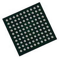
EP3C10M164C8N Altera, EP3C10M164C8N Datasheet - Page 72

EP3C10M164C8N
Manufacturer Part Number
EP3C10M164C8N
Description
IC CYCLONE III FPGA 402MHZ BGA-164
Manufacturer
Altera
Series
Cyclone IIIr
Specifications of EP3C10M164C8N
No. Of Logic Blocks
645
Family Type
Cyclone III
No. Of I/o's
106
I/o Supply Voltage
3.3V
Operating Frequency Max
402MHz
Operating Temperature Range
0°C To +85°C
Family Name
Cyclone III
Number Of Logic Blocks/elements
10320
# I/os (max)
106
Frequency (max)
402MHz
Process Technology
65nm
Operating Supply Voltage (typ)
1.2V
Logic Cells
10320
Ram Bits
423936
Operating Supply Voltage (min)
1.15V
Operating Supply Voltage (max)
1.25V
Operating Temp Range
0C to 85C
Operating Temperature Classification
Commercial
Mounting
Surface Mount
Pin Count
164
Package Type
MBGA
Lead Free Status / RoHS Status
Lead free / RoHS Compliant
Lead Free Status / RoHS Status
Lead free / RoHS Compliant
Available stocks
Company
Part Number
Manufacturer
Quantity
Price
- Current page: 72 of 350
- Download datasheet (8Mb)
5–8
clkena Signals
Figure 5–5. clkena Implementation: Output Enable
Cyclone III Device Handbook, Volume 1
clkin
clkena
clk_out
1
1
The Cyclone III device family supports clkena signals at the GCLK network level.
This allows you to gate-off the clock even when a PLL is used. Upon re-enabling the
output clock, the PLL does not need a resynchronization or re-lock period because the
circuit gates off the clock at the clock network level. In addition, the PLL can remain
locked independent of the clkena signals because the loop-related counters are not
affected.
Figure 5–4
Figure 5–4. clkena Implementation
The clkena circuitry controlling the output C0 of the PLL to an output pin is
implemented with two registers instead of a single register, as shown in
Figure 5–5
signal is sampled on the falling edge of the clock (clkin).
This feature is useful for applications that require low power or sleep mode.
The clkena signal can also disable clock outputs if the system is not tolerant to
frequency overshoot during PLL resynchronization.
shows how to implement the clkena signal.
shows the waveform example for a clock output enable. The clkena
clkena
clkin
Chapter 5: Clock Networks and PLLs in the Cyclone III Device Family
D
Q
clkena_out
© December 2009 Altera Corporation
clk_out
Figure
Clock Networks
5–4.
Related parts for EP3C10M164C8N
Image
Part Number
Description
Manufacturer
Datasheet
Request
R

Part Number:
Description:
CYCLONE II STARTER KIT EP2C20N
Manufacturer:
Altera
Datasheet:

Part Number:
Description:
CPLD, EP610 Family, ECMOS Process, 300 Gates, 16 Macro Cells, 16 Reg., 16 User I/Os, 5V Supply, 35 Speed Grade, 24DIP
Manufacturer:
Altera Corporation
Datasheet:

Part Number:
Description:
CPLD, EP610 Family, ECMOS Process, 300 Gates, 16 Macro Cells, 16 Reg., 16 User I/Os, 5V Supply, 15 Speed Grade, 24DIP
Manufacturer:
Altera Corporation
Datasheet:

Part Number:
Description:
Manufacturer:
Altera Corporation
Datasheet:

Part Number:
Description:
CPLD, EP610 Family, ECMOS Process, 300 Gates, 16 Macro Cells, 16 Reg., 16 User I/Os, 5V Supply, 30 Speed Grade, 24DIP
Manufacturer:
Altera Corporation
Datasheet:

Part Number:
Description:
High-performance, low-power erasable programmable logic devices with 8 macrocells, 10ns
Manufacturer:
Altera Corporation
Datasheet:

Part Number:
Description:
High-performance, low-power erasable programmable logic devices with 8 macrocells, 7ns
Manufacturer:
Altera Corporation
Datasheet:

Part Number:
Description:
Classic EPLD
Manufacturer:
Altera Corporation
Datasheet:

Part Number:
Description:
High-performance, low-power erasable programmable logic devices with 8 macrocells, 10ns
Manufacturer:
Altera Corporation
Datasheet:

Part Number:
Description:
Manufacturer:
Altera Corporation
Datasheet:

Part Number:
Description:
Manufacturer:
Altera Corporation
Datasheet:

Part Number:
Description:
Manufacturer:
Altera Corporation
Datasheet:

Part Number:
Description:
CPLD, EP610 Family, ECMOS Process, 300 Gates, 16 Macro Cells, 16 Reg., 16 User I/Os, 5V Supply, 25 Speed Grade, 24DIP
Manufacturer:
Altera Corporation
Datasheet:


