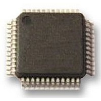
SC16C650BIB48 NXP Semiconductors, SC16C650BIB48 Datasheet - Page 6

SC16C650BIB48
Manufacturer Part Number
SC16C650BIB48
Description
UART, 32BYTE FIFO, 16C650, LQFP48
Manufacturer
NXP Semiconductors
Datasheet
1.SC16C650BIB48151.pdf
(48 pages)
Specifications of SC16C650BIB48
No. Of Channels
1
Data Rate
3Mbps
Supply Voltage Range
2.25V To 5.5V
Operating Temperature Range
-40°C To +85°C
Digital Ic Case Style
LQFP
No. Of Pins
48
Svhc
No SVHC (18-Jun-2010)
Operating
RoHS Compliant
Uart Features
Automatic Software/Hardware Flow Control, Programmable Xon/Xoff Characters
Rohs Compliant
Yes
Available stocks
Company
Part Number
Manufacturer
Quantity
Price
Company:
Part Number:
SC16C650BIB48,151
Manufacturer:
NXP Semiconductors
Quantity:
10 000
Company:
Part Number:
SC16C650BIB48151
Manufacturer:
NXP Semiconductors
Quantity:
135
NXP Semiconductors
Table 2.
SC16C650B_4
Product data sheet
Symbol
D0
D1
D2
D3
D4
D5
D6
D7
DCD
DDIS
DSR
DTR
INT
OUT1
OUT2
OUT
RCLK
IOR
IOR
Pin description
Pin
PLCC44 LQFP48 HVQFN32
2
3
4
5
6
7
8
9
42
26
41
37
33
38
35
-
10
25
24
43
44
45
46
47
2
3
4
40
22
39
33
30
34
31
-
5
20
19
…continued
28
29
30
31
32
1
2
3
-
-
26
22
20
-
-
23
4
-
14
Type
I/O
I/O
I/O
I/O
I/O
I/O
I/O
I/O
I
O
I
O
O
O
O
O
I
I
I
Rev. 04 — 14 September 2009
Description
Data bus. Eight data lines with 3-state outputs provide a
bidirectional path for data, control and status information between
the UART and the CPU.
Data carrier detect. DCD is a modem status signal. Its condition
can be checked by reading MSR[7] (DCD). MSR[3] ( DCD)
indicates that DCD has changed states since the last read from the
MSR. If the modem status interrupt is enabled when DCD changes
levels, an interrupt is generated.
Driver disable. DDIS is active (LOW) when the CPU is reading
data. When inactive (HIGH), DDIS can disable an external
transceiver.
Data set ready. DSR is a modem status signal. Its condition can be
checked by reading MSR[5] (DSR). MSR[1] ( DSR) indicates DSR
has changed levels since the last read from the MSR. If the modem
status interrupt is enabled when DSR changes levels, an interrupt is
generated.
Data terminal ready. When active (LOW), DTR informs a modem
or data set that the UART is ready to establish communication. DTR
is placed in the active level by setting the DTR bit of the Modem
Control Register. DTR is placed in the inactive level either as a
result of a Master Reset, during loopback mode operation, or
clearing the DTR bit.
Interrupt. When active (HIGH), INT informs the CPU that the UART
has an interrupt to be serviced. Four conditions that cause an
interrupt to be issued are: a receiver error, received data that is
available or timed out (FIFO mode only), an empty transmitter
holding register or an enabled modem status interrupt. INT is reset
(deactivated) either when the interrupt is serviced or as a result of a
Master Reset.
Outputs 1 and 2. These are user-designated output terminals that
are set to the active (low) level by setting respective Modem Control
Register (MCR) bits (OUT1 and OUT2). OUT1 and OUT2 are set to
the inactive (HIGH) level as a result of Master Reset, during
loopback mode operations, or by clearing bit 2 (OUT1) or bit 3
(OUT2) of the MCR.
Receiver clock. RCLK is the 16 baud rate clock for the receiver
section of the UART.
Read inputs. When either IOR or IOR is active (LOW or HIGH,
respectively) while the UART is selected, the CPU is allowed to
read status information or data from a selected UART register. Only
one of these inputs is required for the transfer of data during a read
operation; the other input should be tied to its inactive level (i.e.,
IOR tied LOW or IOR tied HIGH).
UART with 32-byte FIFOs and IrDA encoder/decoder
SC16C650B
© NXP B.V. 2009. All rights reserved.
6 of 48


