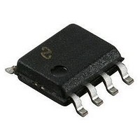
DS36C279M National Semiconductor, DS36C279M Datasheet - Page 9

DS36C279M
Manufacturer Part Number
DS36C279M
Description
IC, RS-485 TRANSCEIVER, 5.25V, SOIC-8
Manufacturer
National Semiconductor
Datasheet
1.DS36C279MNOPB.pdf
(10 pages)
Specifications of DS36C279M
Device Type
Transceiver
Ic Interface Type
RS485
No. Of Drivers
1
Supply Voltage Range
4.75V To 5.25V
Driver Case Style
SOIC
No. Of Pins
8
Operating Temperature Range
-40°C To +85°C
Lead Free Status / RoHS Status
Contains lead / RoHS non-compliant
Available stocks
Company
Part Number
Manufacturer
Quantity
Price
Part Number:
DS36C279M
Manufacturer:
TI/德州仪器
Quantity:
20 000
Company:
Part Number:
DS36C279M/NOPB
Manufacturer:
TI
Quantity:
3 200
Company:
Part Number:
DS36C279MX/NOPB
Manufacturer:
TI
Quantity:
3 200
Part Number:
DS36C279MX/NOPB
Manufacturer:
NS/国半
Quantity:
20 000
Unit Load
A unit load for an RS-485 receiver is defined by the input
current versus the input voltage curve. The gray shaded
region is the defined operating range from −7V to +12V. The
top border extending from −3V at 0 mA to +12V at +1 mA is
defined as one unit load. Likewise, the bottom border ex-
tending from +5V at 0 mA to −7V at −0.8 mA is also defined
as one unit load (see Figure 19). An RS-485 driver is capable
of driving up to 32 unit loads. This allows up to 32 nodes on
a single bus. Although sufficient for many applications, it is
sometimes desirable to have even more nodes. For ex-
ample, an aircraft that has 32 rows with 4 seats per row
would benefit from having 128 nodes on one bus. This would
allow signals to be transferred to and from each individual
seat to 1 main station. Usually there is one or two less seats
in the last row of the aircraft near the restrooms and food
storage area. This frees the node for the main station.
The DS36C278, the DS36C279, and the DS36C280 all have
devices will allow up to 64 nodes or 128 nodes guaranteed
over temperature depending upon which option is selected.
The
the
First, for a
Figure 19 are scaled. Both 0 mA reference points at +5V and
−3V stay the same. The other reference points are +12V at
+0.5 mA for the top border and −7V at −0.4 mA for the
bottom border (see Figure 19). Second, for a
the top and bottom borders shown in Figure 19 are scaled
also. Again, both 0 mA reference points at +5V and −3V stay
the same. The other reference points are +12V at +0.25 mA
for the top border and −7V at −0.2 mA for the bottom border
(see Figure 19).
The advantage of the
increased number of nodes on one bus. In a single master
multi-slave type of application where the number of slaves
exceeds 32, the DS36C278/279/280 may save in the cost of
extra devices like repeaters, extra media like cable, and/or
extra components like resistors.
1
⁄
2
unit load and
1
1
⁄
4
⁄
2
UL is available in commercial temperature.
FIGURE 19. Input Current vs Input Voltage
UL option is available in industrial temperature and
1
⁄
2
UL device the top and bottom borders shown in
1
⁄
4
unit load (UL) options available. These
Operating Range
1
⁄
2
UL and
1
⁄
4
UL devices is the
1
⁄
4
UL device
01205320
9
The DS36C279 and DS36C280 have an additional feature
which offers more advantages. The DS36C279 has an au-
tomatic sleep mode function for power conscious applica-
tions. The DS36C280 has a slew rate control for EMI con-
scious applications. Refer to the sleep mode and slew rate
control portion of the application information section in the
corresponding datasheet for more information on these fea-
tures.
Sleep Mode
The DS36C279 features an automatic shutdown mode that
allows the device to save power when not transmitting data.
Since the shutdown mode is automatic, no external compo-
nents are required. It may be used as little or as much as the
application requires. The more the feature is utilized, the
more power it saves.
The sleep mode is automatically entered when both the
driver and receiver are disabled. This occurs when both the
DE pin is asserted to a logic low and the RE* pin is asserted
to a logic high. Once both pins are asserted the device will
enter sleep mode typically in 50 ns. The DS36C279 is guar-
anteed to go into sleep mode within 600 ns after both pins
are asserted. The device wakes up (comes out of sleep
mode) when either the DE pin is asserted to a logic high
and/or the RE* pin is asserted to a logic low. After the device
enters sleep mode it will take longer for the device to wake
up than it does for the device to enable from TRI-STATE.
Refer to datasheet specifications t
with t
The benefit of the DS36C279 is definitely its power savings.
When active the device has a maximum I
When in sleep mode the device has a maximum I
10 µA, which is 50 times less power than when active. The
I
sleep mode the I
CC
when the device is active is already very low but when in
PZL
and t
PZH
CC
for timing differences.
is ultra low.
PSL
and t
PSH
CC
and compare
www.national.com
of 500 µA.
CC
of only


