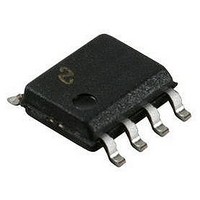
DS36C279M National Semiconductor, DS36C279M Datasheet - Page 4

DS36C279M
Manufacturer Part Number
DS36C279M
Description
IC, RS-485 TRANSCEIVER, 5.25V, SOIC-8
Manufacturer
National Semiconductor
Datasheet
1.DS36C279MNOPB.pdf
(10 pages)
Specifications of DS36C279M
Device Type
Transceiver
Ic Interface Type
RS485
No. Of Drivers
1
Supply Voltage Range
4.75V To 5.25V
Driver Case Style
SOIC
No. Of Pins
8
Operating Temperature Range
-40°C To +85°C
Lead Free Status / RoHS Status
Contains lead / RoHS non-compliant
Available stocks
Company
Part Number
Manufacturer
Quantity
Price
Part Number:
DS36C279M
Manufacturer:
TI/德州仪器
Quantity:
20 000
Company:
Part Number:
DS36C279M/NOPB
Manufacturer:
TI
Quantity:
3 200
Company:
Part Number:
DS36C279MX/NOPB
Manufacturer:
TI
Quantity:
3 200
Part Number:
DS36C279MX/NOPB
Manufacturer:
NS/国半
Quantity:
20 000
www.national.com
RECEIVER CHARACTERISTICS
t
t
t
t
t
t
PLZ
PHZ
PZL
PZH
PSH
PSL
Symbol
Switching Characteristics
Over Supply Voltage and Operating Temperature ranges, unless otherwise specified
Note 3: “Absolute Maximum Ratings” are those values beyond which the safety of the device cannot be guaranteed. They are not meant to imply that the devices
should be operated at these limits. The table of “Electrical Characteristics” specifies conditions of device operation.
Note 4: Current into device pins is defined as positive. Current out of device pins is defined as negative. All voltages are referenced to ground except V
V
Note 5: All typicals are given for: V
Note 6: Delta |V
Note 7: Threshold parameter limits specified as an algebraic value rather than by magnitude.
Note 8: Hysteresis defined as V
Note 9: I
Note 10: C
Note 11: For enable from sleep mode delays DE = L and RE* = H for greater than 600 ns prior to test (device is in sleep mode).
Note 12: For complete details of test, see RS-485.
Parameter Measurement Information
OD2
.
IN
L
includes the receiver input current and driver TRI-STATE leakage current.
Output Disable Time
Output Enable Time
Receiver Enable from Sleep
Mode to Output High
Receiver Enable from Sleep
Mode to Output Low
includes probe and jig capacitance.
FIGURE 1. Driver V
OD2
| and Delta |V
FIGURE 2. Driver V
Parameter
HST
OC
CC
| are changes in magnitude of V
= V
= +5.0V, T
TH
OD2
− V
TL
and V
OD3
A
01205302
.
= + 25˚C.
(Notes 5, 10) (Continued)
OC
C
DE = H
C
(Note 11)
C
(Note 11)
L
L
L
= 15 pF
= 15 pF
= 15 pF
Conditions
01205317
OD2
and V
4
OC
, respectively, that occur when input changes state.
Vtest = −7V to +12V
Figures 14, 15, 16
Figures 14, 16
Figures 14, 15
Reference
FIGURE 3. Driver V
FIGURE 4. Driver I
Min
70
70
OH
Typ
50
55
40
45
97
95
and V
OSD
OL
Max
150
150
150
150
250
250
01205304
01205303
OD1
Units
ns
ns
ns
ns
ns
ns
and


