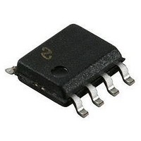
DS36C279M National Semiconductor, DS36C279M Datasheet - Page 2

DS36C279M
Manufacturer Part Number
DS36C279M
Description
IC, RS-485 TRANSCEIVER, 5.25V, SOIC-8
Manufacturer
National Semiconductor
Datasheet
1.DS36C279MNOPB.pdf
(10 pages)
Specifications of DS36C279M
Device Type
Transceiver
Ic Interface Type
RS485
No. Of Drivers
1
Supply Voltage Range
4.75V To 5.25V
Driver Case Style
SOIC
No. Of Pins
8
Operating Temperature Range
-40°C To +85°C
Lead Free Status / RoHS Status
Contains lead / RoHS non-compliant
Available stocks
Company
Part Number
Manufacturer
Quantity
Price
Part Number:
DS36C279M
Manufacturer:
TI/德州仪器
Quantity:
20 000
Company:
Part Number:
DS36C279M/NOPB
Manufacturer:
TI
Quantity:
3 200
Company:
Part Number:
DS36C279MX/NOPB
Manufacturer:
TI
Quantity:
3 200
Part Number:
DS36C279MX/NOPB
Manufacturer:
NS/国半
Quantity:
20 000
www.national.com
Symbol
DIFFERENTIAL DRIVER CHARACTERISTICS
V
V
V
V
∆V
V
V
∆V
I
RECEIVER CHARACTERISTICS
V
V
V
R
I
I
OSD
IN
ING
OD1
OD0
OD0*
OD2
OD3
OC
TH
TL
HST
IN
Absolute Maximum Ratings
If Military/Aerospace specified devices are required,
please contact the National Semiconductor Sales Office/
Distributors for availability and specifications.
Recommended Operating
Conditions
Electrical Characteristics
Over Supply Voltage and Operating Temperature ranges, unless otherwise specified
Supply Voltage (V
Input Voltage (DE, RE*, & DI)
Common Mode (V
Input
Input Voltage (DO/RI,
DO*/RI*)
Supply Voltage (V
Bus Voltage
Operating Free Air Temperature (T
OD2
OC
Driver Output/Receiver
Differential Output Voltage
Output Voltage
Output Voltage
Differential Output Voltage
(Termination Load)
Balance of V
|V
Differential Output Voltage
(Full Load)
Driver Common Mode
Output Voltage
Balance of V
|V
Driver Output Short-Circuit
Current
Differential Input High
Threshold Voltage
Differential Input Low
Threshold Voltage
Hysteresis
Input Resistance
Line Input Current
(Note 9)
Line Input Current Glitch
(Note 9)
OD2
OC
− V
− V
Parameter
OC*
OD2*
CC
CC
CM
|
)
OD2
OC
)
)
|
+4.75
Min
−7
+5.0
Typ
A
)
−0.5V to (V
I
I
(Output to GND)
R
R
R
R1 = 54Ω, R2 = 375Ω
V
R
R
R
R
V
V
V
−7V ≤ V
V
−7V ≤ V
V
−7V ≤ V
Other Input = 0V,
DE = V
V
or 0V
Other Input = 0V,
DE = V
O
O
TEST
O
O
O
O
CM
CC
L
L
L
L
L
L
L
= 0 mA (No Load)
= 0 mA
= 50Ω
= 27Ω
= 27Ω or 50Ω
= 27Ω
= 50Ω
= 27Ω or
= 50Ω
= +12V
= −7V
= V
= V
(Notes 4, 5)
+5.25
= 4.75 to 5.25
Max
= 0V
+12
= −7V to +12V
OH
OL
IL
IL
(Note 3)
CM
CM
CM
, RE* = V
, RE* = V
, I
CC
, I
O
O
≤ +12V
≤ +12V
≤ +12V
Conditions
+0.5V)
Units
= 0.4 mA
= −0.4 mA
±
±
+12V
V
V
15V
14V
IL
IL
,
,
2
DS36C279T
DS36C279
DS36C279
DS36C279T
DS36C279
Receiver Output Voltage
Maximum Package Power Dissipation
derate
Storage Temperature Range
Lead Temperature
DS36C279T
DS36C279
@
M Package 1190 mW,
(Soldering 4 sec)
+25˚C
(422)
(485)
(485)
(422)
(485) Figure 4
V
V
V
Reference
(422, 485)
(422, 485)
(422, 485)
V
V
V
IN
IN
IN
(Note 6)
Figure 2
(Note 6)
(Note 7)
(Note 8)
IN
IN
IN
(422)
(485)
(485)
= +12V
= +12V
= +12V
= −7V
= −7V
= −7V
Figure 1
Figure 1
Min
−40
0
−0.2
−0.2
−0.2
Min
1.5
2.0
1.5
1.5
24
48
0
0
0
0
0
0
0
0
0
0
9.5 mW/˚C above +25˚C
Typ
+25
+25
−0.5V to (V
+0.035
−0.035
−190
0.19
−0.1
0.19
−0.1
0.19
−0.1
Typ
200
2.8
2.3
0.1
2.0
70
68
68
−65˚C to +150˚C
Max
+85
+70
+250
−250
CC
Max
+0.2
+0.2
+0.2
0.25
−0.2
−0.4
0.25
−0.2
5.0
5.0
5.0
5.0
5.0
3.0
3.0
0.5
+260˚C
+0.5V)
Units
˚C
˚C
Units
mA
mA
mV
mA
mA
mA
mA
mA
mA
kΩ
kΩ
V
V
V
V
V
V
V
V
V
V
V
V


