TB6608FNG Toshiba, TB6608FNG Datasheet - Page 20
TB6608FNG
Manufacturer Part Number
TB6608FNG
Description
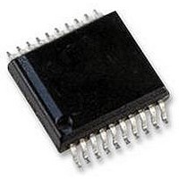
STEPPER MOTOR DRIVE, 13V 0.8A SSOP20
Manufacturer
Toshiba
Datasheet
1.TB6608FNG.pdf
(30 pages)
Specifications of TB6608FNG
No. Of Outputs
2
Output Current
600mA
Output Voltage
15V
Supply Voltage Range
2.7V To 5.5V, 2.5V To 13.5V
Driver Case Style
SSOP
No. Of Pins
20
Operating Temperature Range
-20°C To +85°C
Motor Type
Stepper
Rohs Compliant
Yes
Function
Driver
Vopmax (vm*)
13.5V (15V)
Io (lpeak)
0.6A (0.8A)
Excitation
1/8 step
I/f
CLK input
Mixed Decay Mode
no
Package
SSOP24
Rohs Compatible†
yes
Lead Free Status / RoHS Status
Lead free / RoHS Compliant
Available stocks
Company
Part Number
Manufacturer
Quantity
Price
Company:

Part Number:
TB6608FNG
Manufacturer:
TPT
Quantity:
10 810
Part Number:
TB6608FNG
Manufacturer:
TOSHIBA/东芝
Quantity:
20 000
Company:
Part Number:
TB6608FNG(C8,EL,HJ
Manufacturer:
TI
Quantity:
12


Undervoltage Lockout (UVLO) Circuit
high-impedance state when V
raised to 2.03 V by a hysteresis of 0.03 V.
when ENABLE is set Low. Thus, after the TB6608FNG exits the UVLO mode, the RESET signal should be asserted
for putting the TB6608FNG in the Initial state if necessary.
Electrical Characteristics
(Unless otherwise specified, Ta = 25°C, V
whether they are provided with hysteresis.
The TB6608FNG includes an undervoltage lockout circuit, which puts the output transistors in the
The output transistors are automatically turned on when V
Even when UVLO circuit is tripped, internal circuitry continues to operate in accordance with the CK input like
This table shows which inputs are TTL-compatible and which ones are CMOS-compatible. This also shows
Input voltage
Input hysteresis voltage
Input current
Dynamic supply current
Comparator reference
voltage
Channel-to-channel
voltage differential
Undervoltage lockout
threshold at V
MO output voltage
OSC frequency
CW/CCW, CK, RESET, ENABLE, M1, M2
STBY, TQ, DCY
Characteristics
CC
Input Pins
V
V
V
V
V
V
threshold
threshold
V
V
CC
V
V
Symbol
IN (H) (1)
IN (H) (2)
IN (H) (3)
IN (L) (1)
IN (L) (2)
IN (L) (3)
Lower
Upper
RFA (1)
RFA (2)
RFB (1)
RFB (2)
f
I
I
I
Δ V
V
I
I
OSC
CC1
CC2
CC3
I
I
I
V
INH
INL
M1
M2
M3
MO
decreases to 2.0 V (typ.) or lower.
H
O
,
,
Circuit
UVLD (Design target value)
UVLC (Design target value)
Test
⎯
⎯
⎯
⎯
1
1
1
1
2
3
CW/CCW, CK, RESET, ENABLE, M1, M2
(@ V
CW/CCW, CK, RESET, ENABLE, M1, M2
(@ V
STBY, TQ, DCY
CW/CCW, CK, RESET, ENABLE, M1, M2
V
V
Outputs: Open, ENABLE: H, RESET: H
ENABLE: L
Standby mode
Outputs: Open, ENABLE: H, RESET: H
ENABLE: L
Standby mode
TQ: L, 2-phase excitation
TQ: H, 2-phase excitation
B/A, TQ: L
C
Input Level
I
MO
IN
IN
OSC
CMOS
TTL
= 3.0 V
= GND
CC
CC
CC
= 1 mA
= 220 pF
= 3.3 V)
= 5.5 V)
= 3.3 V, V
20
Test Condition
CC
Hysteresis
increases past the lockout threshold, which is
M
Yes
No
= 5 V, R
NF
= 2 Ω, C
V
0.445
− 0.2
− 0.2
− 0.2
Min
− 11
300
CC
2.8
0.6
0.1
⎯
⎯
⎯
⎯
⎯
⎯
⎯
⎯
⎯
⎯
⎯
2
5
×
OSC
0.125
Typ.
2.03
200
460
0.5
0.5
2.0
15
⎯
⎯
⎯
⎯
⎯
⎯
⎯
⎯
⎯
⎯
4
4
5
1
TB6608FNG
= 220 pF.)
2007-12-17
V
V
V
V
0.555
0.15
0.15
Max
620
CC
0.2
0.8
CC
0.2
0.8
CC
0.2
CC
1.0
0.5
25
10
⎯
11
⎯
⎯
1
6
6
2
1
+
+
+
×
Unit
kHz
mV
mA
mA
mA
mA
μ A
μ A
μ A
μ A
%
V
V
V
V
V
V
V
V
V
V
Related parts for TB6608FNG
Image
Part Number
Description
Manufacturer
Datasheet
Request
R

Part Number:
Description:
Toshiba Semiconductor [TOSHIBA IGBT Module Silicon N Channel IGBT]
Manufacturer:
TOSHIBA Semiconductor CORPORATION
Datasheet:
Part Number:
Description:
TOSHIBA GTR MODULE SILICON NPN TRIPLE DIFFUSED TYPE
Manufacturer:
TOSHIBA Semiconductor CORPORATION
Datasheet:
Part Number:
Description:
TOSHIBA GTR Module Silicon N Channel IGBT
Manufacturer:
TOSHIBA Semiconductor CORPORATION
Datasheet:
Part Number:
Description:
TOSHIBA Intelligent Power Module Silicon N Channel IGBT
Manufacturer:
TOSHIBA Semiconductor CORPORATION
Datasheet:
Part Number:
Description:
TOSHIBA INTELLIGENT POWER MODULE SILICON N CHANNEL LGBT
Manufacturer:
TOSHIBA Semiconductor CORPORATION
Datasheet:
Part Number:
Description:
TOSHIBA IGBT Module Silicon N Channel IGBT
Manufacturer:
TOSHIBA Semiconductor CORPORATION
Datasheet:
Part Number:
Description:
TOSHIBA GTR MODULE SILICON N−CHANNEL IGBT
Manufacturer:
TOSHIBA Semiconductor CORPORATION
Datasheet:
Part Number:
Description:
TOSHIBA Intelligent Power Module Silicon N Channel IGBT
Manufacturer:
TOSHIBA Semiconductor CORPORATION
Datasheet:
Part Number:
Description:
TOSHIBA GTR Module Silicon N Channel IGBT
Manufacturer:
TOSHIBA Semiconductor CORPORATION
Datasheet:
Part Number:
Description:
TOSHIBA INTELLIGENT POWER MODULE
Manufacturer:
TOSHIBA Semiconductor CORPORATION
Datasheet:
Part Number:
Description:
TOSHIBA Intelligent Power Module Silicon N Channel IGBT
Manufacturer:
TOSHIBA Semiconductor CORPORATION
Datasheet:
Part Number:
Description:
TOSHIBA Intelligent Power Module Silicon N Channel IGBT
Manufacturer:
TOSHIBA Semiconductor CORPORATION
Datasheet:
Part Number:
Description:
TOSHIBA IGBT Module Silicon N Channel IGBT
Manufacturer:
TOSHIBA Semiconductor CORPORATION
Datasheet:
Part Number:
Description:
TOSHIBA Intelligent Power Module Silicon N Channel IGBT
Manufacturer:
TOSHIBA Semiconductor CORPORATION
Datasheet:
Part Number:
Description:
Toshiba Semiconductor [SILICON N CHANNEL 1GBT]
Manufacturer:
TOSHIBA Semiconductor CORPORATION
Datasheet: