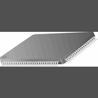
DS90CR483VJD National Semiconductor, DS90CR483VJD Datasheet - Page 14

DS90CR483VJD
Manufacturer Part Number
DS90CR483VJD
Description
IC, LVDS CHANNEL LINK SER/DES, TQFP-100
Manufacturer
National Semiconductor
Datasheet
1.DS90CR483VJD.pdf
(22 pages)
Specifications of DS90CR483VJD
Supply Current
280mA
Supply Voltage Range
3V To 3.6V
Driver Case Style
TQFP
No. Of Pins
100
Operating Temperature Range
-10°C To +70°C
Device Type
Clock
Termination Type
SMD
Filter Terminals
SMD
Rohs Compliant
No
Data Rate Max
5380Mbps
Lead Free Status / RoHS Status
Contains lead / RoHS non-compliant
Available stocks
Company
Part Number
Manufacturer
Quantity
Price
Company:
Part Number:
DS90CR483VJD
Manufacturer:
NS
Quantity:
26
Company:
Part Number:
DS90CR483VJD
Manufacturer:
Texas Instruments
Quantity:
10 000
Company:
Part Number:
DS90CR483VJD/NOPB
Manufacturer:
National Semiconductor
Quantity:
135
Company:
Part Number:
DS90CR483VJD/NOPB
Manufacturer:
Texas Instruments
Quantity:
10 000
Company:
Part Number:
DS90CR483VJDX
Manufacturer:
Texas Instruments
Quantity:
10 000
Company:
Part Number:
DS90CR483VJDX/NOPB
Manufacturer:
Texas Instruments
Quantity:
10 000
www.national.com
Applications Information
The DS90CR483/DS90CR484 chipset is improved over prior
generations of Channel Link devices and offers higher band-
width support and longer cable drive with three areas of
enhancement. To increase bandwidth, the maximum clock
rate is increased to 112 MHz and 8 serialized LVDS outputs
are provided. Cable drive is enhanced with a user selectable
pre-emphasis feature that provides additional output current
during transitions to counteract cable loading effects. This
requires the use of one pull up resistor to Vcc; please refer to
Table 1 to set the level needed. Optional DC balancing on a
cycle-to-cycle basis, is also provided to reduce ISI (Inter-
Symbol Interference). With pre-emphasis and DC balancing,
a low distortion eye-pattern is provided at the receiver end of
the cable. A cable deskew capability has been added to
deskew long cables of pair-to-pair skew of up to
data bit time (up to 80 MHz clock rates). For details on
deskew, refer to “Deskew” section below. These three en-
hancements allow cables 5+ meters in length to be driven
depending upon media and clock rate.
The DS90CR483/484 chipset may also be used in a non-DC
Balance mode. In this mode pre-emphasis is supported. In
Note 10: This is based on testing with standard shield twisted pair cable. The amount of pre-emphasis will vary depending on the type of cable, length and operating
frequency.
2. DC Balance: In addition to data information an additional
bit is transmitted on every LVDS data signal line during each
cycle as shown in Figure 15. This bit is the DC balance bit
(DCBAL). The purpose of the DC Balance bit is to minimize
the short- and long-term DC bias on the signal lines. This is
achieved by selectively sending the data either unmodified
or inverted.
The value of the DC balance bit is calculated from the
running word disparity and the data disparity of the current
word to be sent. The data disparity of the current word shall
be calculated by subtracting the number of bits of value 0
from the number of bits value 1 in the current word. Initially,
the running word disparity may be any value between +7 and
−6. The running word disparity shall be calculated as a
continuous sum of all the modified data disparity values,
where the unmodified data disparity value is the calculated
data disparity minus 1 if the data is sent unmodified and 1
1MΩ or NC
Frequency
112MHz
112MHz
80MHz
80MHz
66MHz
50kΩ
100Ω
Rpre
9kΩ
3kΩ
1kΩ
TABLE 1. Pre-emphasis DC voltage level with (Rpre)
TABLE 2. Pre-emphasis needed per cable length
±
Resulting PRE Voltage
1 LVDS
PRE Voltage
0.75V
1.0V
1.5V
2.0V
2.6V
1.0V
1.5V
1.0V
1.2V
1.5V
Vcc
14
this mode, the chipset is also compatible with 21 and 28-bit
Channel Link Receivers. See Figure 16 for the LVDS map-
ping.
New features Description:
1. Pre-emphasis: Adds extra current during LVDS logic
transition to reduce the cable loading effects. Pre-emphasis
strength is set via a DC voltage level applied from min to max
(0.75V to Vcc) at the “PRE” pin. A higher input voltage on the
”PRE” pin increases the magnitude of dynamic current dur-
ing data transition. The “PRE” pin requires one pull-up resis-
tor (Rpre) to Vcc in order to set the DC level. There is an
internal resistor network, which cause a voltage drop. Please
refer to the tables below to set the voltage level.
The waveshape at the Receiver input should not exhibit over
or undershoot with the proper amount of pre-emphasis set.
Too much pre-emphasis generates excess noise and in-
creases power dissipation. Cables less than 2 meters in
length typically do not require pre-emphasis.
plus the inverse of the calculated data disparity if the data is
sent inverted. The value of the running word disparity shall
saturate at +7 and −6.
The value of the DC balance bit (DCBAL) shall be 0 when
the data is sent unmodified and 1 when the data is sent
inverted. To determine whether to send data unmodified or
inverted, the running word disparity and the current data
disparity are used. If the running word disparity is positive
and the current data disparity is positive, the data shall be
sent inverted. If the running word disparity is positive and the
current data disparity is zero or negative, the data shall be
sent unmodified. If the running word disparity is negative and
the current data disparity is positive, the data shall be sent
unmodified. If the running word disparity is negative and the
current data disparity is zero or negative, the data shall be
sent inverted. If the running word disparity is zero, the data
shall be sent inverted.
Typical cable length
100% pre-emphasis
50% pre-emphasis
Standard LVDS
5+ meters
2 meters
5 meters
2 meters
7 meters
Effect


