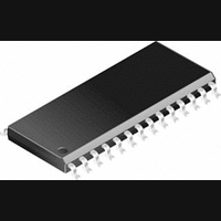
CS4228A-KSZ Cirrus Logic Inc, CS4228A-KSZ Datasheet - Page 16

CS4228A-KSZ
Manufacturer Part Number
CS4228A-KSZ
Description
IC, AUDIO CODEC, 24BIT, 100KHZ, SSOP-28
Manufacturer
Cirrus Logic Inc
Datasheet
1.CS4228A-KSZ.pdf
(30 pages)
Specifications of CS4228A-KSZ
Audio Codec Type
Stereo
No. Of Adcs
2
No. Of Dacs
6
No. Of Input Channels
2
No. Of Output Channels
6
Adc / Dac Resolution
24bit
Adcs / Dacs Signal To Noise Ratio
90dB
Lead Free Status / RoHS Status
Lead free / RoHS Compliant
Available stocks
Company
Part Number
Manufacturer
Quantity
Price
Part Number:
CS4228A-KSZ
Manufacturer:
CIRRUS
Quantity:
20 000
The control port has 2 operating modes: SPI and
I
ates as a slave device. Mode selection is deter-
mined by the state of the SDOUT pin when RST
transitions from low to high: high for SPI, low for
I
sistive load from SDOUT to DGND of less than 47
k will enable I
SPI Mode
In SPI mode, CS is the CS4228 chip select signal,
CCLK is the control port bit clock input, and CDIN
is the input data line. There is no data output line,
therefore all registers are write-only in SPI mode.
Data is clocked in on the rising edge of CCLK.
Figure 13 shows the operation of the control port in
SPI mode. The first 7 bits on CDIN, after CS goes
low, form the chip address (0010000). The eighth
bit is a read/write indicator (R/W), which should be
low to write. The next 8 bits set the Memory Ad-
dress Pointer (MAP) which is the address of the
register that is to be written. The following bytes
contain the data which will be placed into the reg-
isters designated by the MAP.
16
2
2
C compatible. In both modes the CS4228 oper-
C. SDOUT is internally pulled high to VL. A re-
SDIN1/2/3
SDOUT
LRCK
SCLK
MSB
2
One Line Data Mode, Data Valid on Rising Edge of SCLK
Bits/Sample
20
C Mode after a reset.
DAC1
ADCL
20 clks
20 clks
LSB
MSB
DAC3
Left Channel
20 clks
Figure 12. One Line Data Serial Audio Format
64 clks
LSB
SCLK Rate(s)
128 Fs
MSB
DAC5
20 clks
LSB
The CS4228 has a MAP auto increment capability,
enabled by the INCR bit in the MAP register. If
INCR is zero, then the MAP will stay constant for
successive reads or writes. If INCR is 1, then MAP
will increment after each byte is read or written, al-
lowing block reads or writes of successive regis-
ters.
I
In I
is clocked into and out of the port by the SCL clock.
The signal timing is shown in Figure 14. The AD0
pin forms the LSB of the chip address. The upper 6
bits of the 7 bit address field must be 001000. To
communicate with a CS4228, the LSB of the chip
address field, which is the first byte sent to the
CS4228 after a Start condition, should match the
setting of the AD0 pin. The eighth bit of the address
bit is the R/W bit (high for a read, low for a write).
When writing, the next byte is the Memory Ad-
dress Pointer (MAP) which selects the register to
be read or written. If the operation is a read, the
contents of the register pointed to by the MAP will
be output. Setting the auto increment bit in the
MSB
2
C Mode
Notes
6 inputs, 2 outputs, BRM only
2
DAC2
20 clks
20 clks
ADCR
C mode, SDA is a bidirectional data line. Data
LSB
MSB
Right Channel
DAC4
20 clks
64 clks
LSB
MSB
DAC6
20 clks
LSB
CS4228
DS307PP1
MSB


