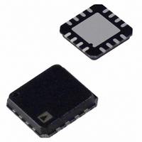
AD8330ACPZ-R2 Analog Devices Inc, AD8330ACPZ-R2 Datasheet - Page 22

AD8330ACPZ-R2
Manufacturer Part Number
AD8330ACPZ-R2
Description
IC, VAR GAIN AMP, 150MHZ, 2DB, LFCSP-16
Manufacturer
Analog Devices Inc
Datasheet
1.AD8330-EVALZ.pdf
(32 pages)
Specifications of AD8330ACPZ-R2
No. Of Amplifiers
1
Bandwidth
150MHz
Gain Accuracy
2dB
Rail To Rail I/o Type
Rail Rail Outputs
No. Of Channels
1
Supply Voltage Range
2.7V To 6V
Amplifier Case Style
LFCSP
Amplifier Type
Variable Gain
Number Of Circuits
1
Output Type
Differential, Rail-to-Rail
Slew Rate
1500 V/µs
-3db Bandwidth
150MHz
Current - Input Bias
100nA
Current - Supply
20mA
Voltage - Supply, Single/dual (±)
2.7 V ~ 6 V
Operating Temperature
-40°C ~ 85°C
Mounting Type
Surface Mount
Package / Case
16-LFCSP
Rohs Compliant
Yes
Lead Free Status / RoHS Status
Lead free / RoHS Compliant
For Use With
AD8330-EVALZ - BOARD EVAL FOR AD8330
Current - Output / Channel
-
Gain Bandwidth Product
-
Voltage - Input Offset
-
Lead Free Status / RoHS Status
Lead free / RoHS Compliant, Lead free / RoHS Compliant
AD8330
Using Single-Sided Sources and Loads
Where the source provides a single-sided output, either INHI
or INLO can be used for the input, with a polarity change when
using INLO. The unused pin must be connected either through
a capacitor to ground, or through a dc bias point that corresponds
closely to the dc level on the active signal pin. The input CMRR
over the full frequency range is illustrated in Figure 59. In some
cases, an additional element such as a SAW filter (having a
single-sided balanced configuration) or a flux-coupled trans-
former can be interposed. Where this element must be terminated
in the correct impedance, other than 1 kΩ, it is necessary to add
either shunt or series resistors at this interface.
When driving a single-sided load, either OPHI or OPLO can be
used. These outputs are very symmetric, so the only effect of
this choice is to select the desired polarity. However, when the
frequency range of interest extends to the upper limits of the
AD8330, a dummy resistor of the same value should be attached
to the unused output. Figure 60 illustrates the ac gain and phase
response for various loads and V
unloaded (C
(20 dB) using only the single-sided output. Adding a 75 Ω load
from OPHI to an ac ground results in Line 2. The gain becomes
a factor of ×1.5 V or 3.54 dB lower, but artifacts of the output
–100
–200
–300
–400
–500
–600
–10
–20
–30
–10
30
20
10
Figure 59. Input CMRR vs. Frequency for Various Values of V
90
80
70
60
50
40
30
20
10
Figure 60. AC Gain and Phase for Various Loading Conditions
0
0
1M
0
50k
V
1
DBS
0
L
0
= 12 pF) case for reference; the gain is 6 dB lower
V
k
DBS
= 0V
= 1.5V
V
DBS
10M
= 0.75V
FREQUENCY (Hz)
FREQUENCY (Hz)
1
M
DBS
= 0.75 V. Line 1 shows the
OFST: ENABLED
10M
100M
DISABLED
LINE 4
LINE 4
LINE 2
LINE 1
LINE 1
LINE 2
LINE 3
LINE 3
500M
1
0
DBS
0
M
Rev. E | Page 22 of 32
common-mode control loop appear in both the magnitude and
phase response.
Adding a dummy 75 Ω to OPLO results in Line 3: the gain is a
further 2.5 dB lower, at about 14 dB. The CM artifacts are no
longer present but a small amount of peaking occurs. If objec-
tionable, this can be eliminated by raising both of the capacitors
on the output pins to 25 pF, as shown in Line 4 of Figure 60.
The gain reduction incurred both by using only one output and
by the additional effect of loading can be overcome by taking
advantage of the VMAG feature, provided primarily for just such
circumstances. Thus, to restore the basic gain in the first case
(Line 1), a 1 V source should be applied to this pin; to restore the
gain in the second case, this voltage should be raised by a factor
of ×1.5 to 1.5 V. In Case 3 and Case 4, a further factor of ×1.33
is needed to make up the 2.5 dB loss, that is, V
raised to 2 V. With the restoration of gain, the peak output
swing at the load is, likewise restored to ±2 V.
Pulse Operation
When using the AD8330 in applications where its transient
response is of greater interest and the outputs are conveyed to
their loads via coaxial cables, the added capacitances can slightly
differ in value, and can be placed either at the sending or load
end of the cables, or divided between these nodes. Figure 61
shows an illustrative example where dual, 1 meter, 75 Ω cables
are driven through dc-blocking capacitors and are independently
terminated at ground level.
Because of the considerable variation between applications,
only general recommendations can be made with regard to
minimizing pulse overshoot and droop. The former can be
optimized by adding small load capacitances, if necessary;
the latter requires the use of sufficiently large capacitors (C1).
VPSI
INHI
INLO
MODE
E
VDBS
N
B
L
VGA CORE
BIAS AND
Figure 61. Driving Dual Cables with Grounded Loads
GAIN INTERFACE
V-REF
OFST
CMGN
OFFSET CONTROL
CM MODE AND
VPOS
COMM
OUTPUT
STAGES
CONTROL
OUTPUT
C
VMAG
NC
N
VPSO
OPHI
OPLO
CMOP
T
CD2
R
CD3
C1
C1
RD2
MAG
CL1
CL2
should be
V
S
2.7V–6V
RL2
RL1


