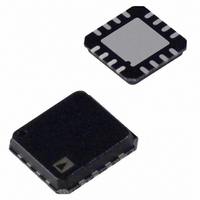
AD8330ACPZ-R2 Analog Devices Inc, AD8330ACPZ-R2 Datasheet - Page 18

AD8330ACPZ-R2
Manufacturer Part Number
AD8330ACPZ-R2
Description
IC, VAR GAIN AMP, 150MHZ, 2DB, LFCSP-16
Manufacturer
Analog Devices Inc
Datasheet
1.AD8330-EVALZ.pdf
(32 pages)
Specifications of AD8330ACPZ-R2
No. Of Amplifiers
1
Bandwidth
150MHz
Gain Accuracy
2dB
Rail To Rail I/o Type
Rail Rail Outputs
No. Of Channels
1
Supply Voltage Range
2.7V To 6V
Amplifier Case Style
LFCSP
Amplifier Type
Variable Gain
Number Of Circuits
1
Output Type
Differential, Rail-to-Rail
Slew Rate
1500 V/µs
-3db Bandwidth
150MHz
Current - Input Bias
100nA
Current - Supply
20mA
Voltage - Supply, Single/dual (±)
2.7 V ~ 6 V
Operating Temperature
-40°C ~ 85°C
Mounting Type
Surface Mount
Package / Case
16-LFCSP
Rohs Compliant
Yes
Lead Free Status / RoHS Status
Lead free / RoHS Compliant
For Use With
AD8330-EVALZ - BOARD EVAL FOR AD8330
Current - Output / Channel
-
Gain Bandwidth Product
-
Voltage - Input Offset
-
Lead Free Status / RoHS Status
Lead free / RoHS Compliant, Lead free / RoHS Compliant
AD8330
Noise, Input Capacity, and Dynamic Range
The design of variable gain amplifiers invariably incurs some
compromises in noise performance. However, the structure of
the AD8330 is such that this penalty is minimal. Examination
of the simplified schematic (Figure 47) shows that the input
voltage is converted to current-mode form by the two 500 Ω
resistors at Pin INHI and Pin INLO, whose combined Johnson
noise contributes 4.08 nV/√Hz. The total input noise at full
gain, when driven from a low impedance source, is typically
5 nV/√Hz after accounting for the voltage and current noise
contributions of the loop amplifier. For a 200 kHz channel
bandwidth, this amounts to 2.24 μV rms. The peak input at full
gain is ±6.4 mV, or +4.5 mV rms for a sine wave signal. The
signal-to-noise ratio at full input, that is, the dynamic range, for
these conditions is, thus, 20 log10(4.5 mV/2.24 μV), or 66 dB.
The value of V
noise, but it is assumed to be 0.5 V.
Below midgain (25 dB, V
section dominates, and the total input noise is 11 nV/√Hz, or
4.9 μV rms in a 200 kHz bandwidth, and the peak input is
78 mV rms. Thus, the dynamic range increases to 84 dB.
At minimum gain, the input noise is up to 120 nV/√Hz, or
53.7 mV rms in the assumed 200 kHz bandwidth, while the
input capacity is ±2 V, or +1.414 V rms (sine), a dynamic range
of 88.4 dB. In calculating the dynamic range for other channel
bandwidths, Δf, subtract 10 log10(Δf/200 kHz) from these
illustrative values. A system operating with a 2 MHz bandwidth,
for example, exhibits dynamic range values that are uniformly
10 dB lower; used in an audio application with a 20 kHz band-
width, they are 10 dB higher.
Noise figure is a misleading metric for amplifiers that are not
impedance matched at their input, which is the special condi-
tion resulting only when both the voltage and current components
of a signal, that is, the signal power, are used at the input port.
When a source of impedance (R
of R
only one of these components is used, either the current (as in
the AD8330) or the voltage. Then, even if the amplifier is
Figure 52. Gain Control Function and Input Referred Noise Spectral Density
S
(a condition that is not to be confused with matching),
100k
–20
–40
–60
10k
100
80
60
40
20
1k
10
0.001
0
1
MAG
has essentially no effect on the input referred
0.01
over a 120 dB Range
DBS
= 0.75 V), noise in the output
V
GAIN
S
0.1
) is terminated using a resistor
(V)
1
10
Rev. E | Page 18 of 32
perfect, the noise figure cannot be better than 3 dB. The 1 kΩ
internal termination resistance would result in a minimum
noise figure of 3 dB for an R
noise-free. However, this is not the case, and the minimum
noise figure occurs at a slightly different value of R
example, see Figure 53 and the Using the AD8330 section).
Dynamic Range
The ratio of peak output swing, expressed in rms terms, to the
output-referred noise spectral density provides a measure of
dynamic range, in dB/√Hz. For a certain class of variable gain
amplifiers, exemplified by the Analog Devices X-AMP® family,
the dynamic range is essentially independent of the gain setting
because the peak output swing and noise are both constant. The
AD8330 provides a different dynamic range profile because
there is no longer a constant relationship between these two
parameters. Figure 54 compares the dynamic range of the
AD8330 to a representative X-AMP.
Figure 53. Noise Figure for Source Resistance of 50 Ω to 5 kΩ, at f = 10 MHz
Figure 54. Dynamic Range in dB/√Hz vs. V
15
14
13
12
11
10
144
140
136
132
128
124
120
116
9
8
7
6
5
10
0 0.1 0.2 0.3 0.4 0.5 0.6 0.7 0.8 0.9 1.0 1.1 1.2 1.3 1.4 1.5
Compared with a Representative X-AMP (Simulation)
X-AMP WITH 40dB
OF GAIN AND AN
INPUT NSD
OF
nV/√Hz
(Lower) and 100 MHz (Simulation)
100
S
of 1 kΩ if the amplifier were
R
V
S
DBS
(Ω)
(V)
CONSTANT 1V rms
OUTPUT, BOTH CASES
DBS
(V
1k
MAG
= 0.5 V, 1 V rms Output)
S
(for an
10k


