SCA3100-D04 VTI Technologies, SCA3100-D04 Datasheet - Page 25
SCA3100-D04
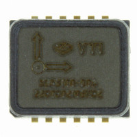
Manufacturer Part Number
SCA3100-D04
Description
ACCELEROMETER 3-AXIS +/-2G SPI
Manufacturer
VTI Technologies
Specifications of SCA3100-D04
Axis
X, Y, Z
Acceleration Range
±2g
Sensitivity
900 counts/g
Voltage - Supply
3 V ~ 3.6 V
Output Type
Digital
Bandwidth
55Hz
Interface
SPI
Mounting Type
Surface Mount
Package / Case
12-SMD
For Use With
551-1061 - EVAL BOARD ACCELEROMETER 3-AXIS551-1056 - KIT DEMO ACCELEROMETER SCA3100
Lead Free Status / RoHS Status
Lead free / RoHS Compliant
Other names
551-1055-2


4.1.2
4.1.3
4.1.3.1
VTI Technologies Oy
www.vti.fi
SPI bus error conditioning
Examples of SPI communication
Example of register read
address for the selected operation, which is defined by bit 7 (‘0’ = read ‘1’ = write), which is
followed by one zero bit. The later 8 bits in the MOSI line contain data for a write operation and are
‘don’t-care’ for a read operation. Bits from MOSI line are sampled in on the rising edge of SCK and
bits to MISO line are latched out on falling edge of SCK.
The first bits in the MISO line are the frame error bit (SPI_FRAME, bit 2) of the previous SPI frame
and odd parity bit (PAR, bit 8). Parity is calculated from data which is currently sent. Bit 7 is always
‘1’. The later 8 bits contain data for a read operation. During the write operation, these data bits are
previous data bits of the addressed register.
For write commands, data is written into the addressed register on the rising edge of CSB. If the
command frame is invalid as described in the section data will not be written into the register
(please see "error conditioning" in section 4.1.2).
For read commands, data is latched into the internal SPI output register (shift register) on the 8th
rising edge of SCK. The output register is shifted out MSB first over MISO output.
When the CSB is high state between data transfers, the MISO line is in the high-impedance state.
While sending an SPI frame, if the CSB is raised to 1
the frame error is activated and the frame is considered invalid. The status bit
STATUS.SPI_FRAME is set to indicate the frame error condition. During the next SPI, the frame
error bit is sent out as SPI_FRAME bit (see SPI_FRAME in MISO line in Figure 6).
STATUS.SPI_FRAME bit is reset, if correct frame is received.
When an invalid frame is received, the last command is simply ignored and the register contents
are left unchanged. If frame error happens while sending multiple samples in ring buffer mode, only
the last output value is considered invalid.
An example of 11 bit X-axis acceleration read command is presented in Figure 7. The master gives
the register address to be read via the MOSI line: '05' in hex format and '000101' in binary format,
register name is X_MSB (X-axis MSB frame). 7
The sensor replies to a requested operation by transferring the register content via MISO line. After
transferring the asked X_MSB register content, the master gives next register address to be read:
'04' in hex format and '000100' in binary format, register name is X_LSB (X-axis LSB frame). The
sensor replies to the requested operation by transferring the register content MSB first.
Figure 7. An example of SPI read communication.
-
-
before sending 16 SCKs or
the number of SCK pulses is not divisible by 8,
Doc.Nr. 8257300A.07
th
bit is set to '0' to indicate the read operation.
SCA3000 Series
Rev.A.07
25/ 43
Related parts for SCA3100-D04
Image
Part Number
Description
Manufacturer
Datasheet
Request
R

Part Number:
Description:
KIT DEMO ACCELEROMETER SCA3100
Manufacturer:
VTI Technologies
Datasheet:

Part Number:
Description:
EVAL BOARD ACCELEROMETER 3-AXIS
Manufacturer:
VTI Technologies
Datasheet:

Part Number:
Description:
ACCELEROMETER 3-AXIS +/-6G SPI
Manufacturer:
VTI Technologies
Datasheet:

Part Number:
Description:
ACCELEROMETER SGL 1.7G DIL8 SMD
Manufacturer:
VTI Technologies
Datasheet:

Part Number:
Description:
VTI Automotive Digital Accelerometer Platform
Manufacturer:
VTI [VTI technologies]
Datasheet:

Part Number:
Description:
BOARD PWB ACCEL 3-AXIS SPI/I2C
Manufacturer:
VTI Technologies
Datasheet:

Part Number:
Description:
EVAL BOARD ACCELEROMETER Y-AXIS
Manufacturer:
VTI Technologies
Datasheet:

Part Number:
Description:
EVAL BOARD INCLINOMETER Y-AXIS
Manufacturer:
VTI Technologies
Datasheet:

Part Number:
Description:
KIT DEMO ACCELEROMTR CMA3000-D01
Manufacturer:
VTI Technologies
Datasheet:

Part Number:
Description:
DEMO KIT WITH SCC1300-D04
Manufacturer:
VTI Technologies
Datasheet:
Part Number:
Description:
ACCELEROMETER SGL 1.7G DIL8 SMD
Manufacturer:
VTI Technologies
Datasheet:
Part Number:
Description:
VTI Automotive Digital Accelerometer Platform
Manufacturer:
VTI [VTI technologies]
Datasheet:
Part Number:
Description:
Accelerometer
Manufacturer:
VTI [VTI technologies]
Datasheet:
Part Number:
Description:
Stand Alone Inclinometer
Manufacturer:
VTI [VTI technologies]
Datasheet:
Part Number:
Description:
3-axis accelerometer
Manufacturer:
VTI [VTI technologies]
Datasheet: