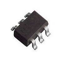
BGU7033,115 NXP Semiconductors, BGU7033,115 Datasheet - Page 4

BGU7033,115
Manufacturer Part Number
BGU7033,115
Description
IC AMPLIFIER MMIC LNA SOT363
Manufacturer
NXP Semiconductors
Type
Monolithic Microwave Integrated Circuit (MMIC)r
Datasheet
1.BGU7033115.pdf
(11 pages)
Specifications of BGU7033,115
Current - Supply
43mA
Frequency
40MHz ~ 1GHz
Gain
10dB
Noise Figure
6dB
P1db
14dBm
Package / Case
6-TSSOP, SC-88, SOT-363
Rf Type
General Purpose
Test Frequency
1GHz
Voltage - Supply
4.75 V ~ 5.5 V
Operating Frequency
1 GHz
Operating Supply Voltage
24 V
Supply Current
43 mA
Maximum Power Dissipation
250 mW
Maximum Operating Temperature
+ 70 C
Mounting Style
SMD/SMT
Minimum Operating Temperature
- 10 C
Number Of Channels
1
Lead Free Status / RoHS Status
Lead free / RoHS Compliant
Other names
568-5508-2
NXP Semiconductors
BGU7033
Product data sheet
Table 7.
T
[1]
[2]
Table 8.
−
Remark: V
Remark: V
Symbol Parameter
FL
RL
RL
P
IP3
V
≤ 0.7
≥ 4.3
≥ 4.3
NF
≤ 0.7
10
amb
L(1dB)
CTRL1
in
out
O
°
Mode depends on setting of V
The fundamental frequency (f
f
2
= 25
C
= f
≤
(V
1
T
± 1 MHz. Input power P
°
ctrl(Gp)
flatness of frequency response
noise figure
input return loss
output return loss
output power at 1 dB gain
compression
output third-order intercept point
amb
C; typical values at V
Characteristics
Gain selection (pins CTRL1, CTRL2)
ctrl(Gp)
ctrl(bp)
≤
) (V)
+70
All information provided in this document is subject to legal disclaimers.
must not exceed V
must not exceed V
°
C; recommended power-up condition: V
Rev. 2 — 13 September 2010
…continued
1
i
CTRL1
) is 1000 MHz. The intermodulation product (IM3) is 2 × f
= −10 dBm.
CC
V
≤ 0.7
≤ 0.7
≥ 4.3
≥ 4.3
CTRL2
= 5 V; Z
and V
CC
CC
(V
1 GHz wideband low-noise amplifier with bypass
CTRL2
; I
; I
ctrl(bp)
S
CTRL2
CTRL1
= Z
Conditions
G
G
bypass mode
G
G
bypass mode
G
G
bypass mode
1 GHz; G
mode
G
G
G
bypass mode
; see
p
p
p
p
p
p
p
p
p
L
) (V)
= 5 dB mode
= 10 dB mode
= 5 dB mode
= 10 dB mode
= 5 dB mode
= 10 dB mode
= 10 dB mode
= 5 dB mode
= 10 dB mode
= 75
must be limited to a maximum of 5 mA.
Table
must be limited to a maximum of 5 mA.
p
Ω
= 5 dB
8.
; R
bias
CTRL1
= 43
Mode
bypass
bypass
G
G
p
p
and V
Ω
[1][2]
[1][2]
[1][2]
= 5 dB
= 10 dB
; 40 MHz
[1]
[1]
[1]
[1]
[1]
[1]
[1]
[1]
[1]
[1]
[1]
CTRL2
Min
-
-
-
-
-
-
-
-
-
-
-
-
-
-
-
BGU7033
© NXP B.V. 2010. All rights reserved.
= logic 0 or < 0.7 V.
≤
Typ
−0.2 -
6.0
4.5
2.5
17
18
8
12
12
8
9
14
29
29
29
2
f
1
− f
≤
1
1000 MHz.
, where
Max Unit
-
-
-
-
-
-
-
-
-
-
-
-
-
-
4 of 11
dB
dB
dB
dB
dB
dB
dB
dB
dB
dB
dBm
dBm
dBm
dBm
dBm


