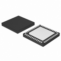
ADP3212MNR2G ON Semiconductor, ADP3212MNR2G Datasheet - Page 8

ADP3212MNR2G
Manufacturer Part Number
ADP3212MNR2G
Description
IC CTLR BUCK 7BIT 2PHASE 48QFN
Manufacturer
ON Semiconductor
Datasheet
1.NCP3218MNR2G.pdf
(35 pages)
Specifications of ADP3212MNR2G
Applications
Controller, Intel IMVP-6.5™
Voltage - Input
3.3 V ~ 22 V
Number Of Outputs
1
Voltage - Output
0.3 V ~ 1.5V
Operating Temperature
-40°C ~ 100°C
Mounting Type
Surface Mount
Package / Case
48-TFQFN Exposed Pad
Output Voltage
0.9512 V
Output Current
52 A
Input Voltage
8 V to 19 V
Supply Current
7 mA
Switching Frequency
300 KHz
Mounting Style
SMD/SMT
Maximum Operating Temperature
+ 100 C
Minimum Operating Temperature
- 40 C
Lead Free Status / RoHS Status
Lead free / RoHS Compliant
Available stocks
Company
Part Number
Manufacturer
Quantity
Price
Company:
Part Number:
ADP3212MNR2G
Manufacturer:
ON Semiconductor
Quantity:
950
Part Number:
ADP3212MNR2G
Manufacturer:
ON/安森美
Quantity:
20 000
ELECTRICAL CHARACTERISTICS
V
V
ZERO CURRENT SWITCHING COMPARATOR
SYSTEM I/O BUFFERS
VID[6:0], DPRSLP, PSI INPUTS
VARFREQ
EN INPUT
PH1, PH0 INPUTS
CLKEN OUTPUT
PWM3, OD3 OUTPUTS
THERMAL MONITORING and PROTECTION
SUPPLY
1. All limits at temperature extremes are guaranteed via correlation using standard statistical quality control (SQC).
2. Guaranteed by design or bench characterization, not production tested.
3. Based on bench characterization data.
4. Timing is referenced to the 90% and 10% points, unless otherwise noted.
Masked Off−Time
Input Voltage
Input Current
VID Delay Time (Note 2)
Input Voltage
Input Current
Input Voltage
Input Current
Input Voltage
Input Current
Output Low Voltage
Output High, Leakage Current
Output Voltage
TTSNS Voltage Range (Note 2)
TTSNS Threshold
TTSNS Hysteresis
TTSNS Bias Current
VRTT Output Voltage
Supply Voltage Range
Supply Current
VCC OK Threshold
VCC UVLO Threshold
CC
VID
= PV
= V
DAC
CC
Parameter
= 5.0 V, FBRTN = PGND = GND = 0 V, H = 5.0 V, L = 0 V, EN = VARFREQ = H, DPRSLP = L, PSI = 1.05 V,
= 1.2000 V, T
A
= −40°C to 100°C, unless otherwise noted. (Note 1) Current entering a pin (sink current) has a positive sign.
t
V
Symbol
OFFMSKD
V
V
CCUVLO
V
CCOK
VRTT
CC
Measured from DRVH1 neg edge to
DRVH1 pos edge at operation max
frequency
Refers to driving signal level
Logic low
Logic high
V = 0.2 V, VID[6:0], DPRSLP
(active pulldown to GND)
PSI (active pullup to VCC)
Any VID edge to FB change 10%
Refers to driving signal level
Logic low
Logic high
Refers to driving signal level
Logic low
Logic high
EN = L or EN = H (static)
0.8 V < EN < 1.6 V (during transition)
Refers to driving signal level
Logic low
Logic high
Logic low, I
Logic high, V
Logic low, I
Logic high, I
VCC = 5.0 V, TTSNS is falling
TTSNS = 2.6 V
Logic low, I
Logic high, I
EN = high
EN = 0 V
VCC is rising
VCC is falling
http://onsemi.com
sink
SINK
VRTT(SINK)
8
SOURCE
VRTT(SOURCE)
CLKEN
Conditions
= 4 mA
= 400 mA
= VCC
= −400 mA
= 400 mA
= −400 mA
2.45
−2.0
Min
200
0.7
4.0
1.9
4.0
4.0
4.5
4.5
4.0
0
Typ
−1.0
4.15
600
−70
1.0
1.0
1.0
5.0
2.5
5.0
4.4
10
60
10
95
10
10
7
Max
2.55
200
100
100
150
0.3
0.7
0.4
0.5
1.0
5.0
2.0
5.5
4.5
10
Units
mV
mV
mV
mV
mA
mA
mA
nA
mA
mA
mA
mA
mA
ns
ns
V
V
V
V
V
V
V
V
V
V
V


