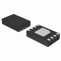
CAT34TS02VP2GT4B ON Semiconductor, CAT34TS02VP2GT4B Datasheet - Page 12

CAT34TS02VP2GT4B
Manufacturer Part Number
CAT34TS02VP2GT4B
Description
IC TEMP SENSOR 2KB MEM 8-TDFN
Manufacturer
ON Semiconductor
Datasheet
1.CAT34TS02VP2GT4A.pdf
(22 pages)
Specifications of CAT34TS02VP2GT4B
Function
Temp Monitoring System (Sensor)
Topology
ADC (Sigma Delta), Comparator, Register Bank
Sensor Type
Internal
Sensing Temperature
-40°C ~ 125°C
Output Type
I²C™, SPI™
Output Alarm
Yes
Output Fan
No
Voltage - Supply
2.97 V ~ 3.63 V
Operating Temperature
-40°C ~ 125°C
Mounting Type
Surface Mount
Package / Case
8-WFDFN Exposed Pad
Digital Output - Bus Interface
I2C, SMBus
Digital Output - Number Of Bits
12 bit
Supply Voltage (min)
3.3 V
Description/function
Digital Output Temperature Sensor with On-board SPD EEPROM
Maximum Operating Temperature
+ 130 C
Minimum Operating Temperature
- 45 C
Supply Current
500 uA
Lead Free Status / RoHS Status
Lead free / RoHS Compliant
Available stocks
Company
Part Number
Manufacturer
Quantity
Price
Company:
Part Number:
CAT34TS02VP2GT4B
Manufacturer:
ON Semiconductor
Quantity:
2 900
Part Number:
CAT34TS02VP2GT4B
Manufacturer:
ON/安森美
Quantity:
20 000
CAT34TS02
SOFTWARE WRITE PROTECTION
The lower half of memory (first 128 bytes) can be
protected against Write requests by setting one of two
Software Write Protection (SWP) flags.
The Permanent Software Write Protection (PSWP)
flag can be set or read while all address pins are at
regular CMOS levels (GND or V
high voltage V
to set, clear or read the Reversible Software Write
Protection (RSWP) flag. The D.C. OPERATING
CONDITIONS for RSWP operations are shown in
Table 1.
The SWP commands are listed in Table 2. All
commands are preceded by a START and terminated
with a STOP, following the ACK or NoACK from the
CAT34TS02. All SWP related Slave addresses use
the pre-amble: 0110 (6h), instead of the regular 1010
(Ah) used for memory access. For PSWP commands,
the three address pins can be at any logic level,
whereas for RSWP commands the address pins must
be at pre-assigned logic levels.
Table 1: RSWP D.C. Operation Condition
Doc. No. MD-1129 Rev. H
Symbol Parameter
ΔV
I
V
HVD
HV
HV
A
A
A
0
0
0
HV
High Voltage Detector Current
Very High Voltage
Overdrive (V
must be present on address pin A0
HV
- V
CC
), whereas the very
CC
)
Test Conditions
1.7 V < V
12
CC
V
must be established on pin A0 before the START
and maintained just beyond the STOP. Otherwise
an RSWP request could be interpreted by the
CAT34TS02 as a PSWP request.
The SWP Slave addresses follow the standard I
convention, i.e. to read the state of the SWP flag, the
LSB of the Slave address must be ‘1’, and to set or
clear a flag, it must be ‘0’. For Write commands a
dummy byte address and dummy data byte must be
provided (Figure 12). In contrast to a regular memory
Read, a SWP Read does not return Data. Instead the
CAT34TS02 will respond with NoACK if the flag is set
and with ACK if the flag is not set. Therefore, the
Master can immediately follow up with a STOP, as
there is no meaningful data following the ACK interval
(Figure 13).
HV
< 3.6 V
is interpreted as logic ‘1’. The V
Min
4.8
7
Characteristics subject to change without notice
© 2010 SCILLC. All rights reserved.
Max
0.1
10
HV
condition
Units
mA
V
V
2
C


