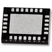
LM25066APSQE/NOPB National Semiconductor, LM25066APSQE/NOPB Datasheet - Page 24

LM25066APSQE/NOPB
Manufacturer Part Number
LM25066APSQE/NOPB
Description
IC CTLR PM HOTSWAP 24-LLP
Manufacturer
National Semiconductor
Series
PowerWise®r
Specifications of LM25066APSQE/NOPB
Applications
Base Station-Networking Line Cards, Servers
Current - Supply
5.8mA
Voltage - Supply
2.9 V ~ 17 V
Operating Temperature
-40°C ~ 85°C
Mounting Type
*
Package / Case
*
Input Voltage
17V
Internal Switch
No
Supply Voltage Range
2.9V To 5.5V
Rohs Compliant
Yes
Digital Ic Case Style
LLP
No. Of Pins
24
Lead Free Status / RoHS Status
Lead free / RoHS Compliant
Other names
LM25066APSQE/NOPBTR
www.national.com
Option D: The OVLO function can be disabled by grounding
the OVLO pin. The UVLO thresholds are set as described in
Option B or Option C.
POWER GOOD
When the voltage at the FB pin increases above its threshold,
the internal pull-down acting on the PGD pin is disabled al-
lowing PGD to rise to V
as shown in
high as 17V and can be higher or lower than the voltages at
VIN and OUT. VDD is a convenient choice for V
lows interface to low voltage logic and avoids glitching on
PGD during power-up. If a delay is required at PGD, suggest-
ed circuits are shown in
C
In
C
R
lows for equal delays at the two edges, or a short delay at the
rising edge and a long delay at the falling edge.
Setting the output threshold for the PGD pin requires two re-
sistors (R4, R5) as shown in
output voltage is shown in
any other voltage which requires monitoring.
The resistor values are calculated as follows:
Choose the upper and lower threshold (V
at V
As an example, assume the application requires the following
thresholds: V
V
R4 = 10 kΩ, R5 = 1.3 kΩ
Where the R4 and R5 resistor values are known, the threshold
voltages and hysteresis are calculated from the following:
PG
PG
PG2
PGD(HYS)
Figure
, while the falling edge is delayed a lesser amount by
OUT
adds delay to the rising edge, but not to the falling edge.
and C
.
15B, the rising edge is delayed by R
= 0.24V. The resistor values are:
PG
Figure
PGDH
. Adding a diode across R
= 10.14V and V
14. The pull-up voltage (V
PGD
Figure
Figure
through the pull-up resistor, R
Figure 13
15. In
13, R4 can be connected to
PGDL
Figure
. While monitoring the
PG2
= 9.9V. Therefore
PGDH
(Figure
PG1
PGD
15A, capacitor
) and (V
PGD
) can be as
+ R
15C) al-
PG2
as it al-
PGDL
and
PG
)
,
24
FIGURE 13. Programming the PGD Threshold
FIGURE 14. Power Good Output
30146051
301460a5


