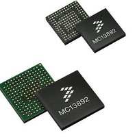
MC13892AJVL Freescale Semiconductor, MC13892AJVL Datasheet - Page 62

MC13892AJVL
Manufacturer Part Number
MC13892AJVL
Description
IC PMU I.MX51/37/35/27 186MAPBGA
Manufacturer
Freescale Semiconductor
Datasheets
1.MC13892AJVLR2.pdf
(156 pages)
2.MC13892AJVLR2.pdf
(2 pages)
3.MC13892AJVLR2.pdf
(16 pages)
4.MC13892AJVLR2.pdf
(5 pages)
Specifications of MC13892AJVL
Applications
Battery Management, Display (LED Drivers), Handheld/Mobile Devices, Power Supply
Operating Temperature
-40°C ~ 85°C
Mounting Type
Surface Mount
Package / Case
186-LFBGA
Mounting Style
SMD/SMT
Duty Cycle (max)
55 %
Input Voltage
- 0.3 V to + 20 V
Maximum Operating Temperature
+ 85 C
Minimum Operating Temperature
- 30 C
Output Current
30 mA
Output Voltage
3.3 V
Topology
Boost
Operating Temperature (max)
85C
Operating Temperature (min)
-40C
Mounting
Surface Mount
Package Type
BGA
Case Length
12mm
Screening Level
Industrial
Lead Free Status / RoHS Status
Lead free / RoHS Compliant
Current - Supply
-
Voltage - Supply
-
Lead Free Status / Rohs Status
Lead free / RoHS Compliant
Available stocks
Company
Part Number
Manufacturer
Quantity
Price
Company:
Part Number:
MC13892AJVL
Manufacturer:
Freescale Semiconductor
Quantity:
10 000
Part Number:
MC13892AJVL
Manufacturer:
FREESCALE
Quantity:
20 000
Company:
Part Number:
MC13892AJVLR2
Manufacturer:
Freescale Semiconductor
Quantity:
10 000
FUNCTIONAL DEVICE OPERATION
OPERATING MODES
TIMING DIAGRAMS
POWER UP
initial delay of 8.0 ms, in which the core circuitry gets enabled. To ensure a proper power up sequence, the outputs of the
switchers are discharged at the beginning of a Cold Start. For that reason, an 8.0 ms delay allows the outputs of the linear
regulators to be fully discharged as well through the built-in discharge path. Time slots which include multiple regulator startups
will be sub-sequenced for additional inrush balancing. The peak inrush current per event is limited. Any under-voltage detection
at BP is masked while the power up sequencer is running.
enabling and output level options are selected by hardwiring the PUMSx pins for the desired configuration. The state of the
PUMSx pins can be read out via the sense bits PUMSSxx[1:0]. Tying the PUMSx pins to ground corresponds to 00, open to 01,
VCOREDIG to 10, and VCORE to 11.
sequestering just the bare essentials, to allow processor startup and software to run. With such a strategy, the startup transients
are controlled at lower levels, and the rest of the system power tree can be brought up by software. This allows optimization of
supply ordering where specific sequences may be required, as well as supply default values. Software code can load up all of
the required programmable options to avoid sneak paths, under/over-voltage issues, startup surges, etc., without any change in
hardware. For this reason, the Power Gate drivers are limited to activation by software rather than the sequencer, allowing the
core(s) to startup before any peripheral loading is introduced.
get enabled.
62
13892
A Turn On event timing diagram example shows in
At power up, switchers and regulators are sequentially enabled in time slots of 2.0 ms steps to limit the inrush current after an
The Power Up mode Select pins (PUMS1 and 2) are used to configure the startup characteristics of the regulators. Supply
The recommended power up strategy for end products is to bring up as little of the system as possible at booting, essentially
The power up defaults
Table 26
Table 25. Timer Main Characteristics
Under-voltage Timer
Reset Timer
Watchdog Timer
Power Cut Timer
shows the initial setup for the voltage level of the switchers and regulators, and whether they
Timer
Figure 12. Power Up Timing Diagram
Figure
4.0 ms
40 ms
128 ms
Programmable 0 to 8 seconds in 31.25 ms steps
12.
Duration
Analog Integrated Circuit Device Data
Freescale Semiconductor


