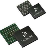
MC13892AJVL Freescale Semiconductor, MC13892AJVL Datasheet - Page 53

MC13892AJVL
Manufacturer Part Number
MC13892AJVL
Description
IC PMU I.MX51/37/35/27 186MAPBGA
Manufacturer
Freescale Semiconductor
Datasheets
1.MC13892AJVLR2.pdf
(156 pages)
2.MC13892AJVLR2.pdf
(2 pages)
3.MC13892AJVLR2.pdf
(16 pages)
4.MC13892AJVLR2.pdf
(5 pages)
Specifications of MC13892AJVL
Applications
Battery Management, Display (LED Drivers), Handheld/Mobile Devices, Power Supply
Operating Temperature
-40°C ~ 85°C
Mounting Type
Surface Mount
Package / Case
186-LFBGA
Mounting Style
SMD/SMT
Duty Cycle (max)
55 %
Input Voltage
- 0.3 V to + 20 V
Maximum Operating Temperature
+ 85 C
Minimum Operating Temperature
- 30 C
Output Current
30 mA
Output Voltage
3.3 V
Topology
Boost
Operating Temperature (max)
85C
Operating Temperature (min)
-40C
Mounting
Surface Mount
Package Type
BGA
Case Length
12mm
Screening Level
Industrial
Lead Free Status / RoHS Status
Lead free / RoHS Compliant
Current - Supply
-
Voltage - Supply
-
Lead Free Status / Rohs Status
Lead free / RoHS Compliant
Available stocks
Company
Part Number
Manufacturer
Quantity
Price
Company:
Part Number:
MC13892AJVL
Manufacturer:
Freescale Semiconductor
Quantity:
10 000
Part Number:
MC13892AJVL
Manufacturer:
FREESCALE
Quantity:
20 000
Company:
Part Number:
MC13892AJVLR2
Manufacturer:
Freescale Semiconductor
Quantity:
10 000
TIME OF DAY ALARM
already on, the processor will be interrupted. The TODA and DAYA registers are used to set the alarm time. Only a single alarm
can be programmed at a time. When the TOD counter is equal to the value in TODA, and the DAY counter is equal to the value
in DAYA, the TODAI interrupt will be generated.
interrupt for the alarm (TODAI) is backed up by LICELL and will be valid at power up. If the mask bit for the TOD alarm (TODAM)
is high, then the TODAI interrupt is masked and the application will not turn on with the time of day alarm event
(TOD[16:0] = TODA[16:0] and DAY[14:0] = DAYA[14:0]). By default, the TODAM mask bit is set to 1, thus masking the interrupt
and turn on event.
TIMER RESET
cell via the LICELL pin. When the backup voltage drops below RTCUVDET, the RTCPORB reset signal is generated and the
contents of the RTC will be reset. Additional registers backed up by coin cell will also reset with RTCPORB. To inform the
processor that the contents of the RTC are no longer valid due to the reset, a timer reset interrupt function is implemented with
the RTCRSTI bit.
RTC TIMER CALIBRATION
registers to comply with digital rights management specifications of ±50 ppm. This calibration system can be disabled, if not
needed to reduce the RTC current drain. The general implementation relies on the system processor to measure the 32.768 kHz
crystal oscillator against a higher frequency and more accurate system clock such as a TCXO. If the RTC timer needs a
correction, a 5 bit 2's complement calibration word can be sent via the SPI to compensate the RTC for inaccuracy in its reference
oscillator as defined in
counter. Therefore, the frequency at the clock outputs CLK32K and CLK32KMCU are not affected.
maximize lifetime when the RTC system is maintained by the coin cell, the RTC Calibration circuitry can be automatically disabled
when main battery contact is lost, or if it is so deeply discharged that RTC power draw is switched to the coin cell (configured
with RTCCALMODE = 01).
down, even after the main battery has discharged. However, it is noted that the calibration can only be as good as the RTCCAL
Analog Integrated Circuit Device Data
Freescale Semiconductor
A Time Of Day Alarm (TODA) function can be used to turn on the application and alert the processor. If the application is
At initial power up of the application (application of the coin cell), the state of the TODA and DAYA registers will be all 1's. The
As long as the supply at BP is valid, the real time clock will be supplied from VCORE. If not, it can be backed up from a coin
A clock calibration system is provided to adjust the 32,768 cycle counter that generates the 1.0 Hz timer for RTC timing
Note that the 32.768 kHz oscillator is not affected by RTCCAL settings. Calibration is only applied to the RTC time base
The RTC system calibration is enabled by programming the RTCCALMODE[1:0] for desired behavior by operational mode.
A slight increase in consumption will be seen when the calibration circuitry is activated. To minimize consumption and
Because of the low RTC consumption, RTC accuracy can be maintained through long periods of the application being shut
Table 19. RTC Calibration Enabling
Table 18. RTC Calibration Settings
Code in RTCCAL[4:0]
Table
RTCCALMODE
18.
00011
00001
00000
10001
10000
01111
11101
11111
00
01
10
11
RTC Calibration disabled (default)
RTC Calibration enabled in all modes except coin cell only
Reserved for future use. Do not use.
RTC Calibration enabled in all modes
Correction in Counts per 32768
+15
-15
-16
+3
+1
-1
-3
0
Function
CLOCK GENERATION AND REAL TIME CLOCK
Relative correction in ppm
FUNCTIONAL DEVICE OPERATION
+458
-458
-488
+92
+31
-31
-92
0
13892
53


