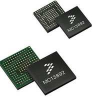
MC13892AJVL Freescale Semiconductor, MC13892AJVL Datasheet - Page 36

MC13892AJVL
Manufacturer Part Number
MC13892AJVL
Description
IC PMU I.MX51/37/35/27 186MAPBGA
Manufacturer
Freescale Semiconductor
Datasheets
1.MC13892AJVLR2.pdf
(156 pages)
2.MC13892AJVLR2.pdf
(2 pages)
3.MC13892AJVLR2.pdf
(16 pages)
4.MC13892AJVLR2.pdf
(5 pages)
Specifications of MC13892AJVL
Applications
Battery Management, Display (LED Drivers), Handheld/Mobile Devices, Power Supply
Operating Temperature
-40°C ~ 85°C
Mounting Type
Surface Mount
Package / Case
186-LFBGA
Mounting Style
SMD/SMT
Duty Cycle (max)
55 %
Input Voltage
- 0.3 V to + 20 V
Maximum Operating Temperature
+ 85 C
Minimum Operating Temperature
- 30 C
Output Current
30 mA
Output Voltage
3.3 V
Topology
Boost
Operating Temperature (max)
85C
Operating Temperature (min)
-40C
Mounting
Surface Mount
Package Type
BGA
Case Length
12mm
Screening Level
Industrial
Lead Free Status / RoHS Status
Lead free / RoHS Compliant
Current - Supply
-
Voltage - Supply
-
Lead Free Status / Rohs Status
Lead free / RoHS Compliant
Available stocks
Company
Part Number
Manufacturer
Quantity
Price
Company:
Part Number:
MC13892AJVL
Manufacturer:
Freescale Semiconductor
Quantity:
10 000
Part Number:
MC13892AJVL
Manufacturer:
FREESCALE
Quantity:
20 000
Company:
Part Number:
MC13892AJVLR2
Manufacturer:
Freescale Semiconductor
Quantity:
10 000
FUNCTIONAL DESCRIPTION
FUNCTIONAL PIN DESCRIPTION
VGEN1DRV
VGEN1
VGEN2DRV
VGEN2
VINGEN3DRV
connected the base of the PNP transistor.
VGEN3
VSRTC
Additionally, it is used to bias the Low Power SRTC domain of the SRTC module integrated on certain FSL processors.
GNDREG1
GNDREG2
GNDREG3
GENERAL OUTPUTS
GPO1
to ADIN5, and one from ADIN5 to GND.
GPO2
GPO3
GPO4
36
13892
Drive output for the VGEN1 external PNP transistor.
Output of general purpose 1 regulator.
Drive output for the VGEN2 external PNP transistor.
Output of general purpose 2 regulator.
1. Input for the VGEN3 regulator when no external PNP transistor used. Typically connected to BP.
2. Drive output for VGEN3 in case an external PNP transistor is used on the application. In this case, this pin must be
Output of general purpose 3 regulator.
Output regulator for the SRTC module on the processor. The VSRTC regulator provides the CLK32KMCU output level (1.2 V).
Ground for regulators 1.
Ground for regulators 2.
Ground for regulators 3.
General purpose output 1. Intended to be used for battery thermistor biasing. In this case, connect a 10 KΩ resistor from GPO1
General purpose output 2.
General purpose output 3.
General purpose output 4. It can be configured for a muxed connection into Channel 7 of the GP ADC.
Analog Integrated Circuit Device Data
Freescale Semiconductor


