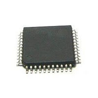
MC56F8255VLD Freescale Semiconductor, MC56F8255VLD Datasheet - Page 20

MC56F8255VLD
Manufacturer Part Number
MC56F8255VLD
Description
DSC 64K FLASH 60MHZ 44-LQFP
Manufacturer
Freescale Semiconductor
Series
56F8xxxr
Datasheets
1.TWR-56F8257.pdf
(88 pages)
2.MC56F8245VLD.pdf
(14 pages)
3.MC56F8245VLD.pdf
(2 pages)
4.MC56F8245VLD.pdf
(629 pages)
Specifications of MC56F8255VLD
Core Processor
56800E
Core Size
16-Bit
Speed
60MHz
Connectivity
CAN, I²C, LIN, SCI, SPI
Peripherals
LVD, POR, PWM, WDT
Number Of I /o
35
Program Memory Size
64KB (32K x 16)
Program Memory Type
FLASH
Ram Size
4K x 16
Voltage - Supply (vcc/vdd)
3 V ~ 3.6 V
Data Converters
A/D 8x12b, D/A 1x12b
Oscillator Type
Internal
Operating Temperature
-40°C ~ 105°C
Package / Case
44-LQFP
Product
DSCs
Processor Series
56800E
Core
56800E
Device Million Instructions Per Second
60 MIPs
Maximum Clock Frequency
60 MHz
Number Of Programmable I/os
35
Data Ram Size
8 KB
Operating Supply Voltage
3.3 V
Maximum Operating Temperature
+ 105 C
Mounting Style
SMD/SMT
Minimum Operating Temperature
- 40 C
On-chip Adc
12 bit, 4 Channel
Lead Free Status / RoHS Status
Lead free / RoHS Compliant
Eeprom Size
-
Lead Free Status / Rohs Status
Details
Available stocks
Company
Part Number
Manufacturer
Quantity
Price
Company:
Part Number:
MC56F8255VLD
Manufacturer:
Freescale Semiconductor
Quantity:
10 000
Signal/Connection Descriptions
20
CMPA_M1)
CMPA_M2)
VREFHA&
VREFLA&
GPIOA2
GPIOA3
GPIOA4
GPIOA5
GPIOA6
GPIOA7
(ANA2&
(ANA3&
(ANA4)
(ANA5)
(ANA6)
(ANA7)
Signal
Name
LQFP
44
10
11
Table 5. MC56F825x/MC56F824x Signal and Package Information (continued)
LQFP
48
11
12
8
LQFP
64
15
16
12
11
10
9
MC56F825x/MC56F824x Digital Signal Controller, Rev. 3
Output
Output
Output
Output
Output
Output
Input/
Input/
Input/
Input/
Input/
Input/
Type
Input
Input
Input
Input
Input
Input
enabled
enabled
enabled
enabled
enabled
enabled
internal
internal
internal
internal
internal
internal
During
Reset
pullup
pullup
pullup
pullup
pullup
pullup
Input,
Input,
Input,
Input,
Input,
Input,
State
Port A GPIO — This GPIO pin can be individually programmed as
an input or output pin.
ANA2 and VREFHA and CMPA_M1 — Analog input to channel 2 of
ADCA and analog references high of ADCA and negative input 1 of
analog comparator A.
When used as an analog input, the signal goes to ANA2 and
VREFHA and CMPA_M1. ADC control register configures this input
as ANA2 or VREFHA.
After reset, the default state is GPIOA2.
Port A GPIO — This GPIO pin can be individually programmed as
an input or output pin.
ANA3 and VREFLA and CMPA_M2 — Analog input to channel 3 of
ADCA and analog references low of ADCA and negative input 2 of
analog comparator A.
When used as an analog input, the signal goes to ANA3 and
VREFLA and CMPA_M2. ADC control register configures this input
as ANA3 or VREFLA.
After reset, the default state is GPIOA3.
Port A GPIO — This GPIO pin can be individually programmed as
an input or output pin.
ANA4 — Analog input to channel 4 of ADCA.
After reset, the default state is GPIOA4.
Port A GPIO — This GPIO pin can be individually programmed as
an input or output pin.
ANA5 — Analog input to channel 5 of ADCA.
After reset, the default state is GPIOA5.
Port A GPIO — This GPIO pin can be individually programmed as
an input or output pin.
ANA6 — Analog input to channel 5 of ADCA.
After reset, the default state is GPIOA6.
Port A GPIO — This GPIO pin can be individually programmed as
an input or output pin.
ANA7 — Analog input to channel 7 of ADCA.
After reset, the default state is GPIOA7.
Signal Description
Freescale Semiconductor


