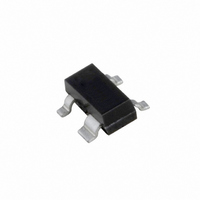
BFG93A/X,215 NXP Semiconductors, BFG93A/X,215 Datasheet - Page 3

BFG93A/X,215
Manufacturer Part Number
BFG93A/X,215
Description
TRANS NPN 12V 35MA 6GHZ SOT143B
Manufacturer
NXP Semiconductors
Datasheet
1.BFG93A215.pdf
(13 pages)
Specifications of BFG93A/X,215
Package / Case
TO-253-4, TO-253AA
Transistor Type
NPN
Voltage - Collector Emitter Breakdown (max)
12V
Frequency - Transition
6GHz
Noise Figure (db Typ @ F)
1.7dB ~ 2.3dB @ 1GHz ~ 2GHz
Power - Max
300mW
Dc Current Gain (hfe) (min) @ Ic, Vce
40 @ 30mA, 5V
Current - Collector (ic) (max)
35mA
Mounting Type
Surface Mount
Dc Collector/base Gain Hfe Min
40
Mounting Style
SMD/SMT
Configuration
Single
Transistor Polarity
NPN
Collector- Emitter Voltage Vceo Max
12 V
Emitter- Base Voltage Vebo
2 V
Continuous Collector Current
35 mA
Power Dissipation
300 mW
Lead Free Status / RoHS Status
Lead free / RoHS Compliant
Gain
-
Lead Free Status / RoHS Status
Lead free / RoHS Compliant, Lead free / RoHS Compliant
Other names
568-6196-2
BFG93A/X,215
BFG93A/X,215
NXP Semiconductors
LIMITING VALUES
In accordance with the Absolute Maximum Rating System (IEC 134).
Note
1. T
THERMAL CHARACTERISTICS
Note
1. T
CHARACTERISTICS
T
Note
1. G
V
V
V
I
P
T
T
R
I
h
C
C
C
f
G
F
SYMBOL
SYMBOL
SYMBOL
C
j
CBO
T
FE
stg
j
CBO
CEO
EBO
tot
th j-s
= 25 C unless otherwise specified.
c
e
re
NPN 6 GHz wideband transistors
UM
s
s
UM
is the temperature at the soldering point of the collector pin.
is the temperature at the soldering point of the collector pin.
is the maximum unilateral power gain, assuming S
collector-base voltage
collector-emitter voltage
emitter-base voltage
collector current (DC)
total power dissipation
storage temperature range
junction operating temperature
thermal resistance from junction to soldering point
collector leakage current
DC current gain
collector capacitance
emitter capacitance
feedback capacitance
transition frequency
maximum unilateral power
gain; note 1
noise figure
PARAMETER
PARAMETER
PARAMETER
open emitter
open base
open collector
T
I
I
I
I
I
I
I
f = 1 GHz
I
f = 2 GHz
T
T
E
C
E
C
C
C
C
C
s
s
amb
s
amb
Rev. 05 - 26 November 2007
= 0; V
= i
= 30 mA; V
= i
= i
= 30 mA; V
= 30 mA; V
= 30 mA; V
=
=
85 C; note 1
e
c
c
= 25 C; f = 1 GHz
= 25 C; f = 2 GHz
opt
opt
= 0; V
= 0; V
= 0; V
CB
; I
; I
C
C
= 5 V
CONDITIONS
CONDITIONS
= 5 mA; V
= 5 mA; V
CB
EB
CB
CE
CE
CE
CE
12
= 5 V; f = 1 MHz
= 5 V; f = 1 MHz
= 5 V; f = 1 MHz
is zero and
= 5 V
= 5 V; f = 500 MHz
= 8 V; T
= 8 V; T
note 1
CONDITIONS
CE
CE
amb
amb
= 8 V;
= 8 V;
G
= 25 C;
= 25 C;
UM
=
10
BFG93A; BFG93A/X
log
40
4.5
MIN.
65
MIN.
-------------------------------------------------------------- dB.
VALUE
1
290
–
S
90
0.9
1.9
0.6
6
16
10
1.7
2.3
TYP.
11
15
12
2
35
300
+150
175
Product specification
S
2
MAX.
21
1
2
50
MAX.
–
S
22
3 of 13
UNIT
K/W
V
V
V
mA
mW
C
C
2
UNIT
nA
pF
pF
pF
GHz
dB
dB
dB
dB
UNIT


