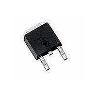
BUK6218-40C,118 NXP Semiconductors, BUK6218-40C,118 Datasheet - Page 8

BUK6218-40C,118
Manufacturer Part Number
BUK6218-40C,118
Description
MOSFET N-CH TRENCH DPAK
Manufacturer
NXP Semiconductors
Series
TrenchMOS™r
Datasheet
1.BUK6218-40C118.pdf
(14 pages)
Specifications of BUK6218-40C,118
Input Capacitance (ciss) @ Vds
1170pF @ 25V
Fet Type
MOSFET N-Channel, Metal Oxide
Fet Feature
Standard
Rds On (max) @ Id, Vgs
16 mOhm @ 10A, 10V
Drain To Source Voltage (vdss)
40V
Current - Continuous Drain (id) @ 25° C
42A
Vgs(th) (max) @ Id
2.8V @ 1mA
Gate Charge (qg) @ Vgs
22nC @ 10V
Power - Max
60W
Mounting Type
Surface Mount
Package / Case
TO-252-3, DPak (2 Leads + Tab), SC-63
Configuration
Single
Transistor Polarity
N-Channel
Resistance Drain-source Rds (on)
18 mOhms
Drain-source Breakdown Voltage
40 V
Gate-source Breakdown Voltage
+/- 20 V
Continuous Drain Current
42 A
Power Dissipation
60 W
Maximum Operating Temperature
+ 175 C
Mounting Style
SMD/SMT
Minimum Operating Temperature
- 55 C
Lead Free Status / RoHS Status
Lead free by exemption / RoHS compliant by exemption
NXP Semiconductors
BUK6218-40C
Product data sheet
Fig 9.
Fig 11. Drain-source on-state resistance as a function
V
R
(m Ω )
GS(th)
(V)
DSon
75
50
25
4
3
2
1
0
0
-60
junction temperature
of drain current; typical values
Gate-source threshold voltage as a function of
0
3.6
3.8
0
20
4.0
max
min
typ
60
V
GS
(V) = 4.5
40
120
All information provided in this document is subject to legal disclaimers.
I
D
003aae848
003aad805
T
(A)
j
10.0
(°C)
5.0
6.0
180
60
Rev. 1 — 4 October 2010
Fig 10. Sub-threshold drain current as a function of
Fig 12. Normalized drain-source on-state resistance
(A)
I
10
D
10
10
10
10
10
a
1.5
0.5
N-channel TrenchMOS intermediate level FET
-1
-2
-3
-4
-5
-6
2
1
0
−60
gate-source voltage
factor as a function of junction temperature
0
0
1
min
BUK6218-40C
60
2
typ
max
120
3
© NXP B.V. 2010. All rights reserved.
003aad806
V
T
GS
j
( ° C)
03aa27
(V)
180
4
8 of 14


