CSBLA455KEC8-B0 Murata, CSBLA455KEC8-B0 Datasheet - Page 23
CSBLA455KEC8-B0
Manufacturer Part Number
CSBLA455KEC8-B0
Description
Resonators 455kHz 0.5%
Manufacturer
Murata
Series
CSBLAr
Datasheets
1.CSBLA400KECE-B0.pdf
(42 pages)
2.CSBLA455KEC8-B0.pdf
(1 pages)
3.CSACS8.00MT-TC.pdf
(21 pages)
Specifications of CSBLA455KEC8-B0
Tolerance
0.5 %
Termination Style
Through Hole
Operating Temperature Range
- 20 C to + 80 C
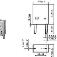
Dimensions
7 mm W x 9 mm L x 3.5 mm H
Frequency Stability
0.3 %
Frequency
455 KHz
Lead Free Status / RoHS Status
Lead free / RoHS Compliant
Available stocks
Company
Part Number
Manufacturer
Quantity
Price
Company:

Part Number:
CSBLA455KEC8-B0
Manufacturer:
MURATA
Quantity:
1 000


!Note
As described in Chapter 2, the most common oscillation
circuit with CERALOCK
circuit with CERALOCK
varies with the application and the IC being used, etc.
Although the basic configuration of the circuit is the
same as that of a quartz crystal, the difference in
mechanical Q results in the difference of the circuit
constant.
This chapter briefly describes the characteristics of the
oscillation circuit and gives some typical examples.
It is becoming more common to configure the oscillation
circuit with a digital IC, and the simplest way to use an
inverter gate.
Fig. 4-1 shows the configuration of a basic oscillation
circuit with a C-MOS inverter.
INV. 1 works as an inverter amplifier of the oscillation
circuit. INV. 2 acts to shape the waveform and also acts
as a buffer for the connection of a frequency counter.
The feedback resistance Rf provides negative feedback
around the inverter in order to put it in the linear
region, so the oscillation will start, when power is
applied.
If the value of Rf is too large, and if the insulation
resistance of the input inverter is accidentally
decreased, oscillation will stop due to the loss of loop
gain. Also, if Rf is too great, noise from other circuits
can be introduced into the oscillation circuit.
Obviously, if Rf is too small, loop gain will be low. An Rf
of 1M is generally used with a ceramic resonator.
Damping resistor Rd provides loose coupling between
the inverter and the feedback circuit and decreases the
loading on the inverter, thus saving energy.
In addition, the damping resistor stabilizes the phase of
the feedback circuit and provides a means of reducing
the gain in the high frequency area, thus preventing the
possibility of spurious oscillation.
Load capacitance C
180°.
The proper selected value depends on the application,
the IC used, and the frequency. If C
are too low, the loop gain in the high frequency is
increased, which in turn increases the probability of
spurious oscillation.
This is particularly likely around 4 to 5 MHz, where the
thickness vibration mode lies, as shown in Fig. 2-5 when
using kHz band resonator.
1. Cautions for Designing Oscillation Circuits
4
Please read rating and !CAUTION (for storage, operating, rating, soldering, mounting and handling) in this PDF catalog to prevent smoking and/or burning, etc.
This catalog has only typical specifications. Therefore, you are requested to approve our product specifications or to transact the approval sheet for product specificaions before ordering.
Applications of Typical Oscillation Circuits
L1
and C
®
®
. The design of the circuit
is to replace L of a Colpitts
L2
provide the phase lag of
L1
and C
L2
values
Fig. 4-1 Basic Oscillation Circuit with C-MOS Inverter
INV.1
C
L1
Rf=1M
IC
X
Rd
C
INV.2
L2
IC
C
L1
V
DD
, C
Rd : Dumping Resistor
IC : 1/6CD4069UBE
L2
X : CERALOCK
Output
: External Capacitance
P17E14.pdf 04.8.24
®
21
4
Related parts for CSBLA455KEC8-B0
Image
Part Number
Description
Manufacturer
Datasheet
Request
R

Part Number:
Description:
Murata Microblower 20x20 DCDC Driver Board - Samples Only
Manufacturer:
Murata
Part Number:
Description:
357-036-542-201 CARDEDGE 36POS DL .156 BLK LOPRO
Manufacturer:
Murata
Datasheet:
Part Number:
Description:
Manufacturer:
Murata
Datasheet:
Part Number:
Description:
Manufacturer:
Murata
Datasheet:
Part Number:
Description:
Manufacturer:
Murata
Datasheet:
Part Number:
Description:
Manufacturer:
Murata
Datasheet:
Part Number:
Description:
Manufacturer:
Murata
Datasheet:
Part Number:
Description:
Manufacturer:
Murata
Datasheet:
Part Number:
Description:
Manufacturer:
Murata
Datasheet:
Part Number:
Description:
BLM21BD751SN1On-Board Type (DC) EMI Suppression Filters
Manufacturer:
Murata
Datasheet:
Part Number:
Description:
BLM15AG100SN1On-Board Type (DC) EMI Suppression Filters
Manufacturer:
Murata
Datasheet:
Part Number:
Description:
NFE31PT222Z1E9On-Board Type (DC) EMI Suppression Filters
Manufacturer:
Murata
Datasheet:
Part Number:
Description:
Chip Coil
Manufacturer:
Murata
Datasheet:
Part Number:
Description:
Chip Coil
Manufacturer:
Murata
Datasheet: