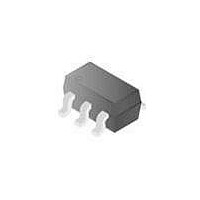
DG9461DV-T1-E3 Vishay, DG9461DV-T1-E3 Datasheet - Page 6

DG9461DV-T1-E3
Manufacturer Part Number
DG9461DV-T1-E3
Description
Analog Switch ICs Low Volt SPDT Switch
Manufacturer
Vishay
Datasheet
1.DG9461DV-T1-E3.pdf
(8 pages)
Specifications of DG9461DV-T1-E3
Number Of Switches
Single
Switch Configuration
SPDT
On Resistance (max)
80 Ohms
On Time (max)
120 ns
Off Time (max)
50 ns
Supply Voltage (max)
12 V
Supply Voltage (min)
2.7 V
Maximum Operating Temperature
+ 85 C
Mounting Style
SMD/SMT
Package / Case
TSOP
Minimum Operating Temperature
- 40 C
Analog Switch Type
SPDT
No. Of Channels
1
On State Resistance Max
30ohm
Turn Off Time
20ns
Turn On Time
35ns
Supply Voltage Range
2.7V To 12V
Operating Temperature Range
-40°C To +85°C
Lead Free Status / RoHS Status
Lead free / RoHS Compliant
Lead Free Status / RoHS Status
Lead free / RoHS Compliant, Lead free / RoHS Compliant
DG9461
Vishay Siliconix
TEST CIRCUITS
www.vishay.com
6
V
V
Logic
Input
NO
NC
V
Switch
gen
Input
NO
NC
IN
C
+
L
C
3 V
R
(includes fixture and stray capacitance)
NO or NC
IN
L
GND
gen
(includes fixture and stray capacitance)
V
OUT
GND
0 V
V+
V+
V+
V+
= V
NC or NO
IN
COM
COM
COM
R
GND
V+
V+
L
+ R
R
L
Switch Output
ON
R
300
COM
R
300
L
L
Ω
Ω
Figure 2. Break-Before-Make Interval
C
35 pF
C
35 pF
L
L
V
OUT
C
V
Figure 3. Charge Injection
Figure 1. Switching Time
L
V
O
OUT
Logic
Input
Switch
Output
V
NC
Output
Switch
= V
Logic
Input
NO
V
V
3 V
0 V
0 V
O
OUT
IN
Logic "1" = Switch On
Logic input waveforms inverted for switches that have
the opposite logic sense.
+ 3 V
0 V
0 V
IN depends on switch configuration: input polarity
determined by sense of switch.
On
90 %
t
D
t
ON
ΔV
Q = ΔV
OUT
50 %
S-71009–Rev. C, 14-May-07
Off
Document Number: 70832
OUT
x C
L
t
D
t
t
t
t
r
r
f
0.9 x V
f
t
On
< 5 ns
< 5 ns
< 20 ns
< 20 ns
OFF
OUT


