DG9461DV-T1-E3 Vishay, DG9461DV-T1-E3 Datasheet
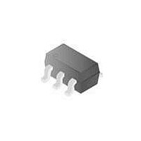
Analog Switch ICs Low Volt SPDT Switch

DG9461DV-T1-E3

Manufacturer Part Number
DG9461DV-T1-E3
Description
Analog Switch ICs Low Volt SPDT Switch
Manufacturer
Vishay
Datasheet

Specifications of DG9461DV-T1-E3

Number Of Switches
Single
Switch Configuration
SPDT
On Resistance (max)
80 Ohms
On Time (max)
120 ns
Off Time (max)
50 ns
Supply Voltage (max)
12 V
Supply Voltage (min)
2.7 V
Maximum Operating Temperature
+ 85 C
Mounting Style
SMD/SMT
Package / Case
TSOP
Minimum Operating Temperature
- 40 C
Analog Switch Type
SPDT
No. Of Channels
1
On State Resistance Max
30ohm
Turn Off Time
20ns
Turn On Time
35ns
Supply Voltage Range
2.7V To 12V
Operating Temperature Range
-40°C To +85°C
Lead Free Status / RoHS Status
Lead free / RoHS Compliant
Lead Free Status / RoHS Status
Lead free / RoHS Compliant, Lead free / RoHS Compliant
DESCRIPTION
The DG9461 is a single-pole/double-throw monolithic CMOS
analog device designed for high performance switching of
analog signals. Combining low power, high speed
(t
and small physical size (TSOP-6), the DG9461 is ideal for
portable and battery powered applications requiring high
performance and efficient use of board space.
The DG9461 is built on Vishay Siliconix’s low voltage
BCD-15 process. Minimum ESD protection, per Method
3015.7, is 2000 V. An epitaxial layer prevents latchup.
Break-before-make is guaranteed for DG9461.
Each switch conducts equally well in both directions when
on, and blocks up to the power supply level when off.
FUNCTIONAL BLOCK DIAGRAM AND PIN CONFIGURATION
* Pb containing terminations are not RoHS compliant, exemptions may apply
Document Number: 70832
S-71009–Rev. C, 14-May-07
ON
: 35 ns, t
OFF
COM
GND
GND
NO
NC
V+
IN
: 20 ns), low on-resistance (r
1
2
3
4
1
2
3
*Not Connected
Low-Voltage Single SPDT Analog Switch
TSOP-6
Top View
Top View
SOIC-8
8
7
6
5
6
5
4
V+
IN
*
*
NO
COM
NC
DS(on)
: 40 Ω)
FEATURES
BENEFITS
APPLICATIONS
Logic "0" ≤ 0.8 V
Logic "1" ≥ 2.4 V
• Low Voltage Operation (+ 2.7 to + 5 V)
• Low On-Resistance - r
• Fast Switching - t
• Low Leakage - I
• Low Charge Injection - Q
• Low Power Consumption
• TTL/CMOS Compatible
• ESD Protection > 2000 V (Method 3015.7)
• Available in TSOP-6 and SOIC-8
• Reduced Power Consumption
• Simple Logic Interface
• High Accuracy
• Reduce Board Space (TSOP-6)
• Battery Operated Systems
• Portable Test Equipment
• Sample and Hold Circuits
• Cellular Phones
• Communication Systems
• Military Radio
• PBX, PABX Guidance and Control Systems
TRUTH TABLE
ORDERING INFORMATION
Temp Range
- 40 to 85 °C
Logic
0
1
COM(on)
ON
: 35 ns, t
Package
DS(on)
TSOP-6
SOIC-8
: 200 pA max
OFF
NC
ON
INJ
: 1 pC
: 40 Ω
OFF
Vishay Siliconix
: 20 ns
DG9461DV-T1-E3
DG9461DY-T1-E3
DG9461DV-T1
DG9461DY-T1
Part Number
DG9461
www.vishay.com
OFF
NO
ON
RoHS*
COMPLIANT
Available
Pb-free
1

Related parts for DG9461DV-T1-E3

DG9461DV-T1-E3 Summary of contents

Page 1

... Logic "0" ≤ 0.8 V Logic "1" ≥ 2.4 V ORDERING INFORMATION Temp Range ° DG9461 Vishay Siliconix : 40 Ω Pb-free DS(on) Available : 35 ns OFF RoHS* : 200 pA max COM(on) COMPLIANT : 1 pC INJ OFF OFF ON Package Part Number DG9461DV-T1 TSOP-6 DG9461DV-T1-E3 DG9461DY-T1 SOIC-8 DG9461DY-T1-E3 www.vishay.com 1 ...

Page 2

... DG9461 Vishay Siliconix ABSOLUTE MAXIMUM RATINGS Parameter Reference V+ to GND a IN, COM, NC, NO Continuous Current (Any terminal) Peak Current (Pulsed duty cycle) ESD (Method 3015.7) Storage Temperature (D Suffix) b Power Dissipation (Packages) Notes: a. Signals exceeding will be clamped by internal diodes. Limit forward diode current to maximum current ratings. ...

Page 3

... V V/1 V COM V/4 V COM NO NC INH 3 Ω nF gen gen = 50 Ω pF MHz MHz DG9461 Vishay Siliconix D Suffix - ° Temp Min Typ Max Full 0 5 Room 30 60 Full 75 Room 0.4 2 Room 2 6 Room - 100 10 100 Full - 5000 5000 Room - 100 10 100 ...

Page 4

... DG9461 Vishay Siliconix TYPICAL CHARACTERISTICS 25 °C, unless otherwise noted 2.0 1 1.0 0.5 0.0 - 0.5 - 1 0.5 1.0 1.5 V COM Charge Injection 100 COM(on 0 Temperature ( Leakage Current vs. Temperature 2.5 2 1.5 1.0 0.5 0.0 - 0.5 - 1.0 - 1.5 - 2 COM Off-Leakage vs. Voltage at 25 °C www ...

Page 5

... OFF 20 0 1.5 2.0 2.5 3 vs. Power Supply Voltage ON OFF Document Number: 70832 S-71009–Rev. C, 14-May-07 2.0 2.5 3.0 COM t ON 3.5 4.0 4.5 5.0 DG9461 Vishay Siliconix OFF Temperature (°C) Switching Time vs. Temperature 2.25 2.00 1.75 1.50 1.25 1.00 0.75 ...

Page 6

... DG9461 Vishay Siliconix TEST CIRCUITS COM Switch Input IN Logic GND Input (includes fixture and stray capacitance OUT COM COM GND C (includes fixture and stray capacitance gen gen 3 V GND www.vishay.com 6 Logic Input Switch Output V OUT Switch Output Ω 300 Figure 1. Switching Time ...

Page 7

... Analyzer 0 V, 2.4 V Vishay Siliconix maintains worldwide manufacturing capability. Products may be manufactured at one of several qualified locations. Reliability data for Silicon Tech- nology and Package Reliability represent a composite of all qualified locations. For related documents such as package/tape drawings, part marking, and reliability data, see http://www.vishay.com/ppg?70832. ...

Page 8

... Vishay disclaims any and all liability arising out of the use or application of any product described herein or of any information provided herein to the maximum extent permitted by law. The product specifications do not expand or otherwise modify Vishay’ ...

Related keywords