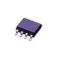
DG419LDY-E3 Vishay, DG419LDY-E3 Datasheet - Page 8

DG419LDY-E3
Manufacturer Part Number
DG419LDY-E3
Description
Analog Switch ICs SPDT Analog Switch
Manufacturer
Vishay
Type
Analog Switchr
Specifications of DG419LDY-E3
Number Of Switches
Single
Switch Configuration
SPDT
On Resistance (max)
70 Ohms
On Time (max)
75 ns
Off Time (max)
41 ns
Supply Voltage (max)
12 V
Supply Voltage (min)
2.7 V
Supply Current
0.00002 mA
Maximum Power Dissipation
400 mW
Maximum Operating Temperature
+ 85 C
Mounting Style
SMD/SMT
Package / Case
SOIC-8 Narrow
Minimum Operating Temperature
- 40 C
Propagation Delay Time
47 ns
Analog Switch Type
SPDT
No. Of Channels
1
On State Resistance Max
18.5ohm
Turn Off Time
32ns
Turn On Time
41ns
Supply Voltage Range
2.7V To 12V
Operating Temperature Range
-40°C To +85°C
Package
8SOIC N
Maximum On Resistance
70@2.7V Ohm
Maximum Propagation Delay Bus To Bus
47@±5V ns
Maximum High Level Output Current
30 mA
Maximum Turn-off Time
41@3V ns
Maximum Turn-on Time
75@3V ns
Switch Architecture
SPDT
Power Supply Type
Single|Dual
Lead Free Status / RoHS Status
Lead free / RoHS Compliant
Lead Free Status / RoHS Status
Lead free / RoHS Compliant, Lead free / RoHS Compliant
Available stocks
Company
Part Number
Manufacturer
Quantity
Price
DG417L/418L/419L
Vishay Siliconix
SCHEMATIC DIAGRAM (TYPICAL CHANNEL)
TEST CIRCUITS
www.vishay.com
8
V
V
Switch
Input
NO
NC
V
IN
GND
V
NO
NC
IN
V
IN
V+
V-
C
C
L
NO or NC
IN
GND
L
L
V
V
V
V
(includes fixture and stray capacitance)
(includes fixture and stray capacitance)
L
L
L
L
V
OUT
GND
= V
IN
V+
V+
V-
V-
COM
V+
V+
V-
V-
COM
R
R
L
L
+ r
R
300 Ω
ON
L
R
300 Ω
L
Switch
Output
C
35 pF
L
Figure 3. Break-Before-Make (DG419L)
V
C
35 pF
Level
Shift/
Drive
OUT
L
Figure 2. Switching Time
V
O
Logic
Input
Switch
Output
Figure 1.
Note:
V
NC
Logic
Input
Switch
Output
Logic input waveform is inverted for switches that
have the opposite logic sense control
= V
V
V
INH
INL
V
NO
0 V
O
V
V
INH
INL
0 V
90 %
V
t
t
D
OUT
ON
50 %
90 %
S-71009–Rev. E, 14-May-07
Document Number: 71763
t
OFF
V-
V+
t
t
r
f
< 5 ns
< 5 ns
S
D
t
0.9 x V
D
t
t
r
f
< 5 ns
< 5 ns
OUT


