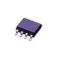
DG419LDY-E3 Vishay, DG419LDY-E3 Datasheet - Page 2

DG419LDY-E3
Manufacturer Part Number
DG419LDY-E3
Description
Analog Switch ICs SPDT Analog Switch
Manufacturer
Vishay
Type
Analog Switchr
Specifications of DG419LDY-E3
Number Of Switches
Single
Switch Configuration
SPDT
On Resistance (max)
70 Ohms
On Time (max)
75 ns
Off Time (max)
41 ns
Supply Voltage (max)
12 V
Supply Voltage (min)
2.7 V
Supply Current
0.00002 mA
Maximum Power Dissipation
400 mW
Maximum Operating Temperature
+ 85 C
Mounting Style
SMD/SMT
Package / Case
SOIC-8 Narrow
Minimum Operating Temperature
- 40 C
Propagation Delay Time
47 ns
Analog Switch Type
SPDT
No. Of Channels
1
On State Resistance Max
18.5ohm
Turn Off Time
32ns
Turn On Time
41ns
Supply Voltage Range
2.7V To 12V
Operating Temperature Range
-40°C To +85°C
Package
8SOIC N
Maximum On Resistance
70@2.7V Ohm
Maximum Propagation Delay Bus To Bus
47@±5V ns
Maximum High Level Output Current
30 mA
Maximum Turn-off Time
41@3V ns
Maximum Turn-on Time
75@3V ns
Switch Architecture
SPDT
Power Supply Type
Single|Dual
Lead Free Status / RoHS Status
Lead free / RoHS Compliant
Lead Free Status / RoHS Status
Lead free / RoHS Compliant, Lead free / RoHS Compliant
Available stocks
Company
Part Number
Manufacturer
Quantity
Price
DG417L/418L/419L
Vishay Siliconix
Notes:
a. Signals on NC, NO, COM, or IN exceeding V+ or V- will be clamped by internal diodes. Limit forward diode current to maximum current ratings.
b. All leads welded or soldered to PC Board.
c. Derate 6.5 mW/°C above 25 °C.
d. Derate 12 mW/°C above 75 °C.
www.vishay.com
2
ABSOLUTE MAXIMUM RATINGS
Parameter
V+ to V-
GND to V-
V
I
Continuous Current (Any Terminal)
Peak Current, S or D (Pulsed 1 ms, 10 % Duty Cycle)
Storage Temperature
Power Dissipation (Packages)
SPECIFICATIONS (SINGLE SUPPLY 12 V)
Parameter
Analog Switch
Analog Signal Range
On-Resistance
Switch Off Leakage Current
Channel On Leakage Current
Digital Control
Input Current
Dynamic Characteristics
Turn-On Time
Turn-Off Time
Break-Before-Make Time Delay
Charge Injection
Off-Isolation
Channel-to-Channel Crosstalk
Source Off Capacitance
Channel-On Capacitance
Power Supplies
Positive Supply Current
Negative Supply Current
Logic Supply Current
Ground Current
N
L
, COM, NC, NO
e
e
a
e
e
e
b
e
I
INL
V
Symbol
I
I
C
C
COM(off)
COM(on)
I
I
ANALOG
OIRR
X
NO(off)
NC(off)
I
t
Q
NO(off)
C
NC(off)
r
t
GND
OFF
TALK
or I
ON
ON
t
I+
I
I-
INJ
ON
D
L
INH
(AK, DQ, DY Suffix)
8-Pin MSOP
8-Pin SOIC
8-Pin CerDIP
R
Unless Otherwise Specified
I
DG419L Only, V
NO
V
L
V
V
V
NO
g
= 50 Ω, C
L
V
, I
NO
R
R
= 0 V, R
= 5 V, V
IN
V+ = 10.8 V, V- = 0 V
, V
NC
L
L
V+ = 12 V, V- = 0 V
V
, V
Test Conditions
= 300 Ω, C
= 300 Ω, C
= 0 or V+, f = 1 MHz
NO
NC
c
V
= 5 mA, V
c
NC
V
COM
d
, V
IN
= 5 V, See Figure 2
g
L
= V
IN
= 0 or V
NC
= 5 pF , f = 1 MHz
= 0 Ω, C
= 1/11 V
= 2.4 V, 0.8 V
COM
= 11/1 V
NC
L
L
COM
, V
= 35 pF
= 35 pF
= 11/1 V
L
NO
L
= 2/9 V
= 1 nF
= 5 V
f
Temp
Room
Room
Room
Room
Room
Room
Room
Room
Room
Room
Room
Room
Room
Room
Room
Room
Full
Full
Full
Full
Full
Full
Full
Full
Full
Full
Full
Full
or 30 mA, whichever occurs first
b
(GND - 0.3) to (V+) + 0.3
- 0.002
- 0.002
- 0.3 to (V+ + 0.3)
0.002
Typ
0.01
0.02
- 71
- 71
13
28
13
13
15
1
5
- 65 to 150
- 0.3 to 13
c
Limit
100
320
400
600
30
7
A Suffix Limits
- 55 to 125 °C
Min
- 1.5
- 7.5
- 7.5
- 15
- 15
- 15
- 1
- 1
- 1
- 1
- 1
0
d
Max
1.5
7.5
7.5
12
20
32
15
15
15
43
50
31
35
1
1
1
1
1
S-71009–Rev. E, 14-May-07
d
Document Number: 71763
D Suffix Limits
Min
- 40 to 85 °C
- 10
- 10
- 10
- 1
- 1
- 1
- 1
- 5
- 1
- 5
- 1
0
d
Max
23.5
12
20
10
10
10
43
46
31
32
1
1
1
1
1
5
1
5
d
Unit
mW
mA
°C
V
Unit
pC
nA
µA
dB
pF
µA
ns
V
Ω


