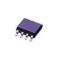
DG419LDY-E3 Vishay, DG419LDY-E3 Datasheet

DG419LDY-E3
Specifications of DG419LDY-E3
Available stocks
Related parts for DG419LDY-E3
DG419LDY-E3 Summary of contents
Page 1
... DG417LDY-T1-E3 DG418LDY DG418LDY-E3 DG418LDY-T1 DG418LDY-T1-E3 DG417LDQ-T1-E3 DG418LDQ-T1-E3 DG417L/418L/419L Vishay Siliconix 14 Ω ON OFF DG419L Dual-In-Line, MSOP-8 and SOIC-8 COM GND Top View OFF Package Part Number DG419LDY DG419LDY-E3 8-Pin Narrow SOIC DG419LDY-T1 DG419LDY-T1-E3 8-Pin MSOP DG419LDQ-T1-E3 www.vishay.com Pb-free Available RoHS* COMPLIANT NO OFF ON 1 ...
Page 2
... DG417L/418L/419L Vishay Siliconix ABSOLUTE MAXIMUM RATINGS Parameter GND COM, NC Continuous Current (Any Terminal) Peak Current (Pulsed 1 ms Duty Cycle) Storage Temperature b Power Dissipation (Packages) Notes: a. Signals on NC, NO, COM exceeding will be clamped by internal diodes. Limit forward diode current to maximum current ratings. b. All leads welded or soldered to PC Board. ...
Page 3
... 300 Ω Room V = ± 3 ± 3 Ω Room Room = 50 Ω MHz L L Room Room MHz Room Room Full Room Full Room Full Room Full DG417L/418L/419L Vishay Siliconix A Suffix Limits D Suffix Limits - 55 to 125 ° ° Min Max Min Max c Typ - 18.5 18 ...
Page 4
... DG417L/418L/419L Vishay Siliconix SPECIFICATIONS (SINGLE SUPPLY 5 V) Parameter Symbol Analog Switch e V Analog Signal Range ANALOG e r On-Resistance ON Dynamic Characteristics e t Turn-On Time Turn-Off Time OFF Break-Before-Make Time Delay e Q Charge Injection INJ Power Supplies e I+ Positive Supply Current e I- Negative Supply Current ...
Page 5
... Full 1.5 V, See Figure 2 Room NO NC Full DG419L Only 1 Room = 300 Ω Ω Room Room = 50 Ω MHz L L Room Room MHz Room DG417L/418L/419L Vishay Siliconix A Suffix Limits D Suffix Limits - 55 to 125 ° ° Min Max Min Max b c Typ 0.005 - 1.5 1 ...
Page 6
... DG417L/418L/419L Vishay Siliconix TYPICAL CHARACTERISTICS 25 °C, unless otherwise noted ° – Analog Voltage (V) COM r vs. V and Supply Voltage ON COM 30 V ± = ± – Analog Voltage (V) COM r vs. Analog Voltage and Temperature 100 µ 10 µ 1 µ 100 100 Input Switching Frequency (Hz) Supply Current vs ...
Page 7
... Switching Threshold vs. Supply Voltage Document Number: 71763 S-71009–Rev. E, 14-May-07 COM(on) /I NC(on ± ± ± OFF - ± OFF - 110 105 125 4.5 5.0 5.5 6.0 DG417L/418L/419L Vishay Siliconix OFF OFF OFF Temperature (°C) Switching Time vs. Temperature and Single Supply Voltage 10 Loss OIRR Ω ...
Page 8
... DG417L/418L/419L Vishay Siliconix SCHEMATIC DIAGRAM (TYPICAL CHANNEL GND V- TEST CIRCUITS Switch Input COM GND V- C (includes fixture and stray capacitance OUT COM GND (includes fixture and stray capacitance) L www.vishay.com 8 Level Shift/ Drive Figure 1. Logic Input Switch Output V OUT 300 Ω Switch ...
Page 9
... Switch Output Figure 4. Transition Time (DG419L dependent on switch configuration Input polarity determined by sense of switch. V- Figure 5. Charge Injection Ω 2 OUT GND V OUT V IN Figure 6. Crosstalk (DG419L) DG417L/418L/419L Vishay Siliconix INH INL t t TRANS TRANS OFF Δ COM 50 Ω www.vishay.com < < ΔV ...
Page 10
... Vishay Siliconix TEST CIRCUITS Vishay Siliconix maintains worldwide manufacturing capability. Products may be manufactured at one of several qualified locations. Reliability data for Silicon Tech- nology and Package Reliability represent a composite of all qualified locations. For related documents such as package/tape drawings, part marking, and reliability data, see http://www ...
Page 11
... Vishay disclaims any and all liability arising out of the use or application of any product described herein or of any information provided herein to the maximum extent permitted by law. The product specifications do not expand or otherwise modify Vishay’ ...


