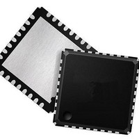
ispPAC-POWR607-01SN32I Lattice, ispPAC-POWR607-01SN32I Datasheet - Page 4

ispPAC-POWR607-01SN32I
Manufacturer Part Number
ispPAC-POWR607-01SN32I
Description
Supervisory Circuits Prec Prog Pwr Supply Seq Mon IND
Manufacturer
Lattice
Type
Power Supply Sequencer and Monitorr
Series
ispPAC®r
Datasheet
1.ISPPAC-POWR607-01SN32I.pdf
(28 pages)
Specifications of ispPAC-POWR607-01SN32I
Internal Hysteresis
Yes
Minimum Operating Temperature
- 40 C
Output Type
Open Collector / Drain
Power Fail Detection
Yes
Number Of Voltages Monitored
6
Monitored Voltage
Adj V
Undervoltage Threshold
Adj
Overvoltage Threshold
Adj
Manual Reset
Resettable
Watchdog
Yes
Power-up Reset Delay (typ)
100 us
Supply Voltage (max)
3.96 V
Supply Voltage (min)
2.64 V
Supply Current (typ)
3.5 mA
Mounting Style
SMD/SMT
Maximum Operating Temperature
+ 85 C
Package / Case
QFN-32
Applications
General Purpose
Voltage - Input
-0.3 V ~ 5.9 V
Voltage - Supply
2.64 V ~ 3.96 V
Current - Supply
3.5mA
Operating Temperature
-40°C ~ 85°C
Mounting Type
Surface Mount
Lead Free Status / RoHS Status
Lead free / RoHS Compliant
Available stocks
Company
Part Number
Manufacturer
Quantity
Price
Company:
Part Number:
ISPPAC-POWR607-01SN32I
Manufacturer:
LATTICE
Quantity:
284
Part Number:
ISPPAC-POWR607-01SN32I
Manufacturer:
LATTICE
Quantity:
20 000
Lattice Semiconductor
Absolute Maximum Ratings
Absolute maximum ratings are shown in the table below. Stresses beyond those listed may cause permanent dam-
age to the device. Functional operation of the device at these or any other conditions beyond those indicated in the
recommended operating conditions of this specification is not implied.
Recommended Operating Conditions
Analog Specifications
I
I
I
1. Includes currents on both V
2. In power-down mode, VCCJ is internally pulled to GND to turn off the JTAG I/O pins. It is important, therefore, that the VCCJ pin be open
3. Leakage measured in power-down mode with applied pin voltages as follows: VCC = 3.96V; IN1_PWRDN, GND = 0V; IN2, VMONx and
V
V
V
V
V
T
T
I
V
V
V
V
V
T
T
1. The die pad on the bottom of the QFN/QFNS package does not need to be electrically or thermally connected to ground.
CC
CCJ
CC_PWRDN
SINKMAX
A
APROG
A
S
CC
CCJ
IN
MON
TRI
OUT
CC
CCJ
IN
MON
Symbol
whenever power-down mode is initiated. If connected to a power supply during power-down mode, VCCJ will draw approximately 2.2mA.
IN_OUTx = 5.5V; HVOUTx configured as FET drivers (HVOUTx configured as open drain outputs have minor leakage path to ground and
are not counted in total); VCCJ, TDI, TDO, TMS and TCK = open.
1
2
Symbol
Symbol
3
Supply current
Supply current
Power-down mode supply current
Core supply
JTAG logic supply
Digital input voltage (all digital I/O pins)
V
Voltage applied to tri-stated pins
Storage temperature
Ambient temperature
Maximum sink current on any output
Core supply voltage at pin
JTAG logic supply voltage at pin
Input voltage at digital input pins
Input voltage at V
Open-drain output voltage
Ambient temperature during
programming
Ambient temperature
MON
Parameter
CC
input voltage
pins.
Parameter
Parameter
MON
pins
ICC + pin leakage currents
Conditions
4-4
HVOUT[1:2] pins in open-
IN_OUT[3:7] pins
Power applied
Conditions
drain mode
(Note 1)
IN_OUT[3:7]
HVOUT[1:2]
Conditions
2
1
Min.
ispPAC-POWR607 Data Sheet
Min.
2.64
2.25
Min.
-0.3
-0.3
-0.3
-0.3
-0.5
-0.5
-0.5
-0.5
-0.5
-0.5
-40
-40
-65
-65
Typ.
3.5
Max.
Max.
3.96
10.4
150
125
4.5
3.6
5.5
5.9
5.5
Max.
85
85
11
23
6
6
6
6
10
5
1
Units
Units
Units
mA
o
o
o
o
mA
mA
V
V
V
V
V
V
µA
V
V
V
V
V
V
C
C
C
C


