L6230PD STMicroelectronics, L6230PD Datasheet
L6230PD
Specifications of L6230PD
Available stocks


Related parts for L6230PD


L6230PD Summary of contents
Page 1
... BLDC motor driving ■ Sinusoidal / 6-steps driving ■ Field oriented control driving system Table 1. Device summary Order codes L6230PD L6230PDTR L6230Q L6230QTR October 2010 This is preliminary information on a new product now in development or undergoing evaluation. Details are subject to change without notice ° ...
Page 2
Contents Contents 1 Block diagram . . . . . . . . . . . . . . . . . . . . . . . . . . . . . . . . . . . ...
Page 3
L6230 1 Block diagram Figure 1. Block diagram Doc ID 18094 Rev 1 Block diagram 3/24 ...
Page 4
Electrical data 2 Electrical data 2.1 Absolute maximum ratings Table 2. Absolute maximum ratings Symbol Parameter V Supply voltage S Differential voltage between: VSA, V OUT1, OUT2, SENSEA and VSB, OD OUT3, SENSEB V Bootstrap peak voltage BOOT V , ...
Page 5
L6230 2.3 Thermal data Table 4. Thermal data Symbol R Maximum thermal resistance junction-ambient th(j-amb)1 R Maximum thermal resistance junction-ambient th(j-amb)1 R Maximum thermal resistance junction-ambient th(j-amb)2 R Maximum thermal resistance junction-ambient th(j-amb)3 1. Mounted on a multi-layer FR4 PCB ...
Page 6
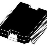
Pin connection 3 Pin connection Figure 2. Pin connection PowerSO36 (top view) Figure 3. Pin connection VFQFPN32 (top view) Note: The pins are connected to die PAD. The die PAD must be connected to GND pin. 6/24 ...
Page 7
L6230 Table 5. Pin description Pin Type VBOOT Power supply Bootstrap voltage needed for driving the upper power MOSFETs. VCP Output Logic DIAG-EN output/input IN1 Logic input EN1 Logic input IN2 Logic input EN2 Logic input IN3 Logic input EN3 ...
Page 8
Electrical characteristics 4 Electrical characteristics ( °C, unless otherwise specified Table 6. Electrical characteristics Symbol Parameter V Turn-on threshold Sth(ON) V Turn-off threshold Sth(OFF) I Quiescent supply current S T Thermal shutdown ...
Page 9
L6230 Table 6. Electrical characteristics (continued) Symbol Parameter Comparator V Offset voltage on sense comparator OFFSET t Turn OFF propagation delay prop t Internal blanking time on comparator blank I Inputs bias current BIAS R Open drain ON resistance CPOUT ...
Page 10
Electrical characteristics Figure 5. Overcurrent detection timing definition 10/24 I OUT I SOVER ON BRIDGE OFF V DIAG-EN 90% 10 OCD(ON) OCD(OFF) Doc ID 18094 Rev 1 L6230 D02IN1387 ...
Page 11
L6230 5 Circuit description 5.1 Power stages and charge pump The L6230 integrates a three-phase bridge, which consists of 6 power MOSFETs connected as shown on the block diagram (see = 0.73 Ω (typical value @ 25 °C) with intrinsic ...
Page 12
Circuit description 5.2 Logic inputs Pins INx and ENx are TTL/CMOS and microcontroller compatible logic inputs. The internal structure is shown in respectively V th(ON) Pin DIAG-EN has identical input structure with the exception that the drain of the Overcurrent ...
Page 13
L6230 5.3 Non-dissipative overcurrent detection and protection The L6230 integrates an overcurrent detection circuit (OCD) for full protection. This circuit provides output-to-output and output-to-ground short circuit protection as well. With this internal over current detection, the external current sense resistor ...
Page 14
Circuit description Figure 11. Overcurrent protection waveforms Figure 12. t DISABLE Figure 13. t DELAY 14/24 I OUT I SOVER DIAG- th(ON) V th(OFF) ON OCD OFF ON t BRIDGE DELAY OFF OCD(ON) EN(FALL) ...
Page 15
L6230 6 Application information Some typical applications using L6230 are shown in this paragraph. A high quality ceramic capacitor ( the range of 100 nF to 200 nF should be placed between the power pins 2 VS and ...
Page 16
Application information The uncommitted internal comparator with open-drain output is available. Figure 14. F.O.C. typical application 6.2 Six-step driving method with current control In this configuration only one sense resistor are needed, the three OUT pins are connected together to ...
Page 17
L6230 Figure 15. Six-step with current control typical application 6.3 Six-step driving method with BEMF zero crossing detection The BEMF zero crossing information can be used to evaluate the rotor position; in this way no Hall effect sensors or encoder ...
Page 18
Application information Figure 16. Six-step with zero crossing detection typical application 6.4 Thermal management In most applications the power dissipation in the IC is the main factor that sets the maximum current that can be delivered by the device in ...
Page 19
L6230 7 Package mechanical data In order to meet environmental requirements, ST offers these devices in different grades of ECOPACK® packages, depending on their level of environmental compliance. ECOPACK® specifications, grade definitions and product status are available at: www.st.com. ECOPACK® ...
Page 20
Package mechanical data Figure 17. Package dimensions 20/24 Doc ID 18094 Rev 1 L6230 ...
Page 21
L6230 Table 10. PowerSO36 mechanical data ( ( Min. Typ. 0.1 0 0.22 0.23 15.8 9.4 13.9 0.65 11.05 ...
Page 22
Package mechanical data Figure 18. PowerSO36 mechanical drawings 22/24 Doc ID 18094 Rev 1 L6230 ...
Page 23
L6230 8 Revision history Table 11. Document revision history Date 14-Oct-2010 Revision 1 First release Doc ID 18094 Rev 1 Revision history Changes 23/24 ...
Page 24
... Information in this document is provided solely in connection with ST products. STMicroelectronics NV and its subsidiaries (“ST”) reserve the right to make changes, corrections, modifications or improvements, to this document, and the products and services described herein at any time, without notice. All ST products are sold pursuant to ST’s terms and conditions of sale. ...