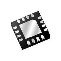
MD1813K6-G Supertex, MD1813K6-G Datasheet - Page 4

MD1813K6-G
Manufacturer Part Number
MD1813K6-G
Description
MOSFET & Power Driver ICs High Speed Quad
Manufacturer
Supertex
Type
High Side/Low Sider
Datasheet
1.MD1813K6-G.pdf
(6 pages)
Specifications of MD1813K6-G
Rise Time
6 ns
Fall Time
6 ns
Supply Voltage (min)
4.5 V
Supply Current
7 mA
Maximum Power Dissipation
2200 mW
Maximum Operating Temperature
+ 85 C
Mounting Style
SMD/SMT
Minimum Operating Temperature
- 20 C
Number Of Drivers
4
Number Of Outputs
4
Package / Case
QFN-16
Lead Free Status / RoHS Status
Lead free / RoHS Compliant
Available stocks
Company
Part Number
Manufacturer
Quantity
Price
Company:
Part Number:
MD1813K6-G
Manufacturer:
Supertex
Quantity:
1 837
Application Information
For proper operation of the MD1813, low inductance bypass
capacitors should be used on the various supply pins. The
GND pin should be connected to the logic ground. The
INA, INB, INC, IND and OE pins should be connected to
a logic source with a swing of GND to VCC, where VCC
is 1.8 to 5.0 volts. Good trace practices should be followed
corresponding to the desired operating speed. The internal
circuitry of the MD1813 is capable of operating up to
100MHz, with the primary speed limitation being the loading
effects of the load capacitance. Because of this speed and
the high transient currents that result with capacitive loads,
the bypass capacitors should be as close to the chip pins
as possible. Unless the load specifically requires bipolar
drive, the VSS, and VL pins should have low inductance
feed-through connections directly to a ground plane. If these
voltages are not zero, then they need bypass capacitors in
a manner similar to the positive power supplies. The power
connections VDD should have a ceramic bypass capacitor
to the ground plane with short leads and decoupling
components to prevent resonance in the power leads.
Output drivers, OUTA and OUTC, drive the gate of an external
P-channel MOSFET, while output drivers OUTB and OUTD
drive the gate of an external N-channel MOSFET, and they
all swing from VH to VL. The auxiliary output drive, OUTG,
swings from VSS to VNEG, and drives the external P-channel
MOSFET as negative bias via a 2KΩ series resistor.
The voltages of VH and VL decide the output signal levels.
These two pins can draw fast transient currents of up to
2.0A, so they should be provided with an appropriate bypass
capacitor located next to the chip pins. A ceramic capacitor
of up to 1.0µF may be appropriate, with a series ferrite bead
Timing Diagram and V
OUTPUT
INPUT
3.3V
12V
0V
0V
Supertex inc.
50%
t
PLH
10%
t
r
TH
90%
●
/ V
1235 Bordeaux Drive, Sunnyvale, CA 94089
50%
OE
Curve
t
PHL
90%
t
f
10%
4
to prevent resonance in the power supply lead coming to
the capacitor. Pay particular attention to minimizing trace
lengths, current loop area, and using sufficient trace width
to reduce inductance. Surface mount components are highly
recommended. Since the output impedance of this driver is
very low, in some cases it may be desirable to add a small
series resistance in series with the output signal to obtain
better waveform transitions at the load terminals. This will of
course reduce the output voltage slew rate at the terminals
of a capacitive load.
The OE pin sets the threshold level of logic for inputs (V
+ V
regardless of the inputs INA or INB. This pin will not control
OUTC, OUTD, or OUTG.
Pay particular attention that parasitic couplings are minimized
from the output to the input signal terminals. The parasitic
feedback may cause oscillations or spurious waveform
shapes on the edges of signal transitions. Since the input
operates with signals down to 1.8V, even small coupled
voltages may cause problems. Use of a solid ground plane
and good power and signal layout practices will prevent this
problem. Be careful that a circulating ground return current
from a capacitive load cannot react with common inductance
to cause noise voltages in the input logic circuitry. Best timing
performance is obtained for OUTC when the voltage of (V
V
When input logic is high, output will swing to VL, and when
input logic is low, output will swing to VH. All inputs must be
kept low until the device is powered up.
NEG
GND
) = (V
) / 2. When OE is low, OUTA is at VH. OUTB is at VL,
V
TH
H
2.0
1.5
1.0
0.5
-V
0
●
0
L
Tel: 408-222-8888
).
1.0
V
TH
2.0
vs V
0.6V
●
www.supertex.com
3.0
OE
V
OE/2
4.0
5.0
MD1813
V
OE
SS
OE
-


