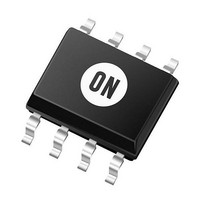
NCP3125ADR2G ON Semiconductor, NCP3125ADR2G Datasheet - Page 2

NCP3125ADR2G
Manufacturer Part Number
NCP3125ADR2G
Description
DC/DC Switching Converters 4A PWM Switching Buck Regulator
Manufacturer
ON Semiconductor
Datasheet
1.NCP3125ADR2G.pdf
(22 pages)
Specifications of NCP3125ADR2G
Mounting Style
SMD/SMT
Duty Cycle (max)
80 %
Efficiency
93 %
Input / Supply Voltage (max)
13.2 V
Input / Supply Voltage (min)
4.5 V
Maximum Operating Temperature
+ 125 C
Minimum Operating Temperature
- 40 C
Operating Temperature Range
- 40 C to + 125 C
Output Current
4 A
Output Voltage
Adjustable
Supply Current
10 mA
Switching Frequency
350 KHz
Package / Case
SOIC-8
Lead Free Status / RoHS Status
Lead free / RoHS Compliant
Available stocks
Company
Part Number
Manufacturer
Quantity
Price
Part Number:
NCP3125ADR2G
Manufacturer:
ON/安森美
Quantity:
20 000
COMP
Table 1. PIN DESCRIPTION
FB
Pin
1
2
3
4
5
6
7
8
VREF
Pin Name
0.8 V
COMP
PGND
AGND
ISET
VSW
BST
VIN
FB
−
+
−
+
AGND
The PGND pin is the high current ground pin for the low−side MOSFET and the drivers. The pin should be
soldered to a large copper area to reduce thermal resistance.
Inverting input to the Operational Transconductance Amplifier (OTA). The FB pin in conjunction with the
external compensation, serves to stabilize and achieve the desired output voltage with voltage mode
control.
COMP pin is used to compensate the OTA which stabilizes the operation of the converter stage. Place
compensation components as close to the converter as possible.
The AGND pin serves as small−signal ground. All small−signal ground paths should connect to the AGND
pin at a single point, avoiding any high current ground returns.
Supply rail for the floating top gate driver. To form a boost circuit, use an external diode to bring the desired
input voltage to this pin (cathode connected to BST pin). Connect a capacitor (CBST) between this pin and
the VSW pin. Typical values for CBST range from 1 nF to 10 nF. Ensure that CBST is placed near the IC.
The VIN pin powers the internal control circuitry and is monitored by an undervoltage comparator. The VIN
pin is also connected to the internal power NMOSFET switches. The VIN pin has high dI/dt edges and must
be decoupled to PGND pin close to the pin of the device.
Current set pin and bottom gate MOSFET driver. Place a resistor to ground to set the current limit of the
converter.
The VSW pin is the connection of the drain and source of the internal N−MOSFETs. The VSW pin swings
from V
dV/dt transitions.
Ramp
IN
10 mA
Clock
OSC
OSC
when the high side switch is on to small negative voltages when the low side switch is on with high
+
−
Comp
PWM
Figure 3. NCP3125 Block Diagram
Fault
VREG
CIRCUIT DESCRIPTION
Count
Latch
Logic
&
http://onsemi.com
Latch
UVLO
POR
R
S
Counter
PWM
OUT
−
+
2
−
+
0.7 V
SCP
Q
DtoA
Description
Fault
Fault
+
−
+
−
VOCTH
+
−
−
+
2 V
BST
VCC
ISET
PGND
VIN
VSW


