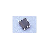
IES5502D Hendon Semiconductors, IES5502D Datasheet - Page 2

IES5502D
Manufacturer Part Number
IES5502D
Description
Buffers & Line Drivers 2.7-5.5V 6.1mA 45ns 400kHz
Manufacturer
Hendon Semiconductors
Datasheet
1.IES5502D.pdf
(11 pages)
Specifications of IES5502D
Logic Family
IE5502
Number Of Channels Per Chip
Dual
Supply Voltage (max)
5.5 V
Supply Voltage (min)
2.7 V
Maximum Operating Temperature
85 C
Mounting Style
SMD/SMT
Minimum Operating Temperature
- 40 C
Supply Current
6.1 mA
Logic Type
Bidirectional Bus Buffer
Package / Case
MSOP-8L
Lead Free Status / RoHS Status
Lead free / RoHS Compliant
5
5.1
6
6.1
The IES5502 can be driven from voltage supplies ranging
from 2.7 V to 5.5 V. The threshold level below which the
output will begin to match the input is 33% of V
the operating voltage should be chosen with the required
bus voltage, switching threshold, and noise margins, in
mind.
6.2
The two buffers (S
symmetrical. The buffers can be driven from either
direction, with the same buffering response. However, the
hot insertion logic is determined from the “backplane”
(S
S
another device on the bus, the other side (e.g. S
be driven low by the IC to provide the buffered output.
The “control” or “input” side is determined by the lowest
externally driven signal. Therefore if the “input” is
externally pulled to V
externally pulled to V
“output” down further such that it becomes
V
subsequently become lower than the “input” by means of
an external device pulling it low (V
the buffering operation will switch sides. The voltage at the
“input” will then become V
2011 Jan 14, Revision 1.5
xx-B
Sxx-C
xx-B
PINNING INFORMATION
FUNCTIONAL DESCRIPTION
) of the buffer is being driven low (<0.3V
) sides of the buffers. When the one side of (e.g.
Fig.2 Pinning diagram (SO8)
= V
Pinning layout
V
S
inputs/outputs
CC
CL-B
S
GND
S
Sxx-B
CL-C
, GND - DC supply pins
CL-B
EN
, S
CL-C
+ V
1
2
3
4
CL
OFFSET
, S
Sxx-C
Sxx-B
and S
DA-B
IES5502
. Should the “output”
= 500 mV, the buffer will pull the
Sxx-B
= 250 mV, and the “output” is
, S
DA
DA-C
) are identical and
= V
Sxx-C
- Buffer
Sxx-C
< V
8
7
6
5
pin5502-8
+ V
Sxx-B
V
S
S
RDY
OFFSET
CC
DA-C
DA-B
CC
), control of
CC
) by
xx-C
. Hence,
. Many
) will
2
Fast Dual Bi-Directional Bus Buffer
5.2
*For device family compatability, please note:
Backplane Side is equivalent to SCL
Card Side is equivalent to SCL
bus buffers are prone to causing glitches during control
transition, but the IES5502 shows negligible glitching even
under the worst operating conditions.
6.3
The enable input (EN) is used to disable the buffer, for the
purpose of isolating sections of the bus. The IC should only
be disabled when the bus is idle, to prevent truncation of
commands which may confuse other devices on the bus.
Upon receiving a valid Enable signal, the IC will wait to
detect either a bus STOP condition, or an IDLE condition
as described in the I
This ensures that truncated transmissions are not
communicated along the newly enabled bus segment.
Enable may be used to progressively activate sections of
the bus during system start-up. Bus sections slow to
respond on power-up can be kept isolated from the main
system to avoid interference and collisions.
The Enable pin may be pulled up higher than the Vcc of the
buffer, further enhancing the capability of the IES5502 in a
level shifting role. For example, a microprocessor could
drive Enable, S
S
Similarly, the threshold level of the Enable pin allows a
1.8V device to enable an IES5502 with a V
(1) “UM10204: I2C-bus Specification and User Manual”, Rev 03,
(2) “System Management Bus (SMBus) Specification”, Version
EN
S
S
GND
RDY
S
S
V
CL-C
SYMBOL
CL-C
CL-B
DA-B
DA-C
CC
19 June 2007, NXP B.V.
2.0, August 3, 2000, SBS Implementers Forum.
and S
Pin description
Enable (EN) - Activate Buffer Operations
DA-C
1
2
3
4
5
6
7
8
CL-B
with Hot Insertion Logic
PIN
ports are at 3.3V.
and S
2
C
(1)
Enable
SCL Buffer, Card* Side
SCL Buffer, Backplane* Side
Supply Ground
Ready
SDA Buffer, Backplane* Side
SDA Buffer, Card* Side
Positive supply
and SMBus
DA-B
at 5V, while the buffer V
OUT
DESCRIPTION
Product Specification
/ SDA
IES5502
IN
(2)
/ SDA
specifications.
OUT
CC
IN
of 3.3V.
CC
,


