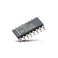
IES5507T Hendon Semiconductors, IES5507T Datasheet - Page 3

IES5507T
Manufacturer Part Number
IES5507T
Description
Buffers & Line Drivers Buffered 4-Chan Bus Switch
Manufacturer
Hendon Semiconductors
Datasheet
1.IES5507T.pdf
(13 pages)
Specifications of IES5507T
Logic Family
IES5507
Number Of Channels Per Chip
4
Supply Voltage (max)
7 V
Supply Voltage (min)
- 0.3 V
Maximum Operating Temperature
+ 85 C
Minimum Operating Temperature
- 40 C
Output Current
30 mA
Output Voltage
110 mV, 80 mV
Supply Current
0.1 uA
Lead Free Status / RoHS Status
Lead free / RoHS Compliant
Available stocks
Company
Part Number
Manufacturer
Quantity
Price
Company:
Part Number:
IES5507T
Manufacturer:
Hendon Semiconductors
Quantity:
135
At some points during the communication, the data
direction will reverse - for example, when the Slave
transmits an acknowledge (ACK) or responds with it’s
register contents. During these times, the controlling
“input” side will have to rise to V
“lock”, which then allows the “output” side to gain control,
and pull (what was) the “input” side low again. This will
cause a “pulse” on the “input” side, which can be quite
large in high capacitance buses. However, this pulse will
not interfere with the actual data transmission, as it should
not occur during times of clock line transition (during
normal I
set-up time requirements are still met.
6.5
The active low RESET input is used to disable the buffer,
and reset it to it’s default state. The IC should only be
disabled when the bus is idle to avoid truncation of
commands which may confuse other devices on the bus.
The RESET signal will clear the contents of the control
register, which has the effect of disabling all output lines
SC0..3 and SD0..3. It is the nature of the I
devices may become ‘stuck’. To help in the clearing of this
condition, the IES5507 can be reset, and each port
brought on-line sucessively to find the component holding
the bus low.
6.6
During power-on, the IES5507 is internally held in the reset
condition for a maximum of t
condition after reset is for the Control Register to be
Erased (all zeros), resulting in all output channels being
disabled.
6.7
The slave address of the IES5507 is shown in the Figure
3. The address pins (A2..0) must be driven to a HIGH or
LOW level - they are not internally pulled to a default state.
2009 Mar 05, Revision 1.0
RESET - Reset IC to Default State
Power On Reset (POR)
A0, A1, A2 - Address lines
2
C and SMBus protocols), and thus data signal
5507-add
1
Fixed Bits
1
Fig.3 Slave Address
1
Externally Selectable Bits
0
RST
A2
LK
= 500ns. The default
A1 A0 R/W
before it releases the
Write = 0
Read = 1
2
C protocol that
Buffered 4-Channel 2-Wire Bus Switch
3
The read/write bit must be set LOW to enable a write to the
control register, or HIGH to read from the control register.
6.8
The control register of the IES5507 is shown in the Figure
4. Each of the four output channels (SCx/SDx pairs) can
be enabled independently, and the direction of the clock
signal can be reversed.
A LOW or zero bit (B3..0) indicates that the respective
channel (SC3..0 / SD3..0) is disabled. The default reset
condition of the register is all zeros, all channels disabled,
forward direction. A HIGH or one bit indicates the
respective channel is enabled.
Example: B3 = 1, B2 = 0, B1 = 1, B0 = 0 means channels
3 (SC3/SD3) and 1 (SC1/SD1) are enabled, and channels
2 (SC2/SD2) and 0 (SC0/SD0) are disabled.
As each channel is individually buffered, the loads on each
are isolated, and therefore there is no special requirement
to keep the sum of the collective capacitances below the
maximum bus capacitance. Instead, each line may have
up to the maximum bus capacitance and be enabled or
disabled without affecting the performance of the other
channels.
The Most Significant Bit (MSB) B7 is used to set the
direction of the SCL (clock) signal. The default state is
LOW (zero). In this state, the SCL port will act as the input,
and the IC will supply a buffered signal to any of the four
output channels (SC0..3) which are enabled. When B7 is
set HIGH (one), the clock signal direction is reversed. The
ports SC0..3 act as inputs, the AND-ed combination of
their signals is buffered and output on the SCL pin.
MSB
0: SCL => SC0..3
1: SC0..3 => SCL
SCL Direction
Control Register
B7
X
Fig.4 Control Register
X
X
B3
Output channel
enable bits
Product Specification
B2 B1 B0
IES5507
5507-reg
LSB


