2N6661 Supertex, 2N6661 Datasheet
2N6661
Specifications of 2N6661
Available stocks


Related parts for 2N6661


2N6661 Summary of contents
Page 1
... MOS devices. Characteristic of all MOS structures, this device is free from thermal runaway and thermally-induced secondary breakdown. Supertex’s vertical DMOS FETs are ideally suited to a wide range of switching and amplifying applications where very low threshold voltage, high breakdown voltage, high input impedance, low input capacitance, and fast switching speeds are desired ...
Page 2
... Reverse recovery time rr Notes: 1. All D.C. parameters 100% tested All A.C. parameters sample tested. Switching Waveforms and Test Circuit 10V INPUT 10 (ON d(ON) VDD 10% OUTPUT 0V 90% Supertex inc. ● Power Dissipation I D (pulsed (A) (W) 3.0 6. 25°C unless otherwise specified) A Min Typ ...
Page 3
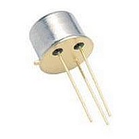
... JEDEC Registration TO-39. * This dimension is not specified in the JEDEC drawing. Drawings not to scale. Supertex Doc. #: DSPD-3TO39N2, Version B052009. (The package drawing(s) in this data sheet may not reflect the most current specifications. For the latest package outline information go to http://www.supertex.com/packaging.html.) does not recommend the use of its products in life support applications, and will not knowingly sell them for use in such applications unless it receives Supertex inc ...