SST5485-E3 Vishay, SST5485-E3 Datasheet
SST5485-E3
Specifications of SST5485-E3


Related parts for SST5485-E3


SST5485-E3 Summary of contents
Page 1
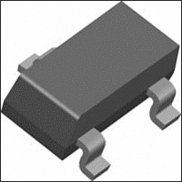
... Packaging Information). 2N/SST5484 Series Vishay Siliconix 2N5484 SST5484 2N5485 SST5485 2N5486 SST5486 APPLICATIONS D High-Frequency Amplifier/Mixer D Oscillator D Sample-and-Hold D Very Low Capacitance Switches TO-236 (SOT- Top View SST5484 (H4)* SST5485 (H5)* SST5486 (H6)* *Marking Code for TO-236 www.vishay.com 1 ...
Page 2
... Series Vishay Siliconix ABSOLUTE MAXIMUM RATINGS Gate-Drain, Gate-Source Voltage . . . . . . . . . . . . . . . . . . . . . . . . . . . . . . . Gate Current . . . . . . . . . . . . . . . . . . . . . . . . . . . . . . . . . . . . . . . . . . . . . . . . . Lead Temperature . . . . . . . . . . . . . . . . . . . . . . . . . . . . . . . . . . . . . . . . . . . . Storage Temperature . . . . . . . . . . . . . . . . . . . . . . . . . . . . . . . . . . . SPECIFICATIONS FOR 2N SERIES (T Parameter Symbol Static Gate-Source V (BR)GSS Breakdown Voltage Gate-Source Cutoff Voltage V GS(off) b Saturation Drain Current I DSS Gate Reverse Current Gate Reverse Current I I GSS ...
Page 3
... MHz 0 kHz 100 MHz 100 MHz 400 MHz 2 2N/SST5484 Series Vishay Siliconix Limits SST5484 SST5485 SST5486 Min Max Min Max Min Max Unit −25 −25 −25 −0.3 −3 −0.5 −4 −2 − −1 −1 −1 −200 −200 −200 www.vishay.com V V ...
Page 4
... Series Vishay Siliconix TYPICAL CHARACTERISTICS (T Drain Current and Transconductance vs. Gate-Source Cutoff Voltage 20 I DSS DSS kHz 0 0 −2 −4 −6 V − Gate-Source Cutoff Voltage (V) GS(off) Gate Leakage Current 100 0 125_C 100 0 25_C 0 − Drain-Gate Voltage (V) DG Output Characteristics −2 V GS(off) ...
Page 5
... S-50148—Rev. G, 24-Jan-05 = 25_C UNLESS OTHERWISE NOTED −1.6 − kHz −1.6 −2 100 80 60 − 2N/SST5484 Series Vishay Siliconix Transfer Characteristics V = − GS(off −55_C A 25_C 125_C 0 −0.6 −1.2 −1.8 −2.4 V − Gate-Source Voltage (V) GS Transconductance vs. Gate-Source Voltage V = − GS(off kHz T = −55_C A 25_C 125_C 0 − ...
Page 6
... Series Vishay Siliconix TYPICAL CHARACTERISTICS (T Common-Source Input Capacitance vs. Gate-Source Voltage MHz −4 −8 −12 V − Gate-Source Voltage (V) GS Input Admittance 100 T = 25_C Common Source 10 1 0.1 100 200 f − Frequency (MHz) Reverse Admittance 25_C Common Source 1 0.1 0.01 100 200 f − ...
Page 7
... Frequency (Hz) Vishay Siliconix maintains worldwide manufacturing capability. Products may be manufactured at one of several qualified locations. Reliability data for Silicon Technology and Package Reliability represent a composite of all qualified locations. For related documents such as package/tape drawings, part marking, and reliability data, see http://www.vishay.com/ppg?70246. ...
Page 8
... Vishay disclaims any and all liability arising out of the use or application of any product described herein or of any information provided herein to the maximum extent permitted by law. The product specifications do not expand or otherwise modify Vishay’ ...