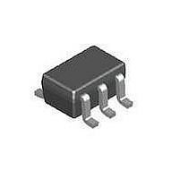
BC847BPDW1T1G ON Semiconductor, BC847BPDW1T1G Datasheet - Page 16

BC847BPDW1T1G
Manufacturer Part Number
BC847BPDW1T1G
Description
Bipolar Small Signal 100mA 50V Dual Complementary
Manufacturer
ON Semiconductor
Datasheet
1.BC847BPDW1T1G.pdf
(17 pages)
Specifications of BC847BPDW1T1G
Dc Collector/base Gain Hfe Min
150 at 10 uA at 5 V
Minimum Operating Temperature
- 55 C
Configuration
Dual
Transistor Polarity
NPN/PNP
Mounting Style
SMD/SMT
Package / Case
SC-70-6
Collector- Emitter Voltage Vceo Max
45 V
Emitter- Base Voltage Vebo
6 V at NPN, 5 V at PNP
Continuous Collector Current
0.1 A
Maximum Dc Collector Current
0.1 A
Power Dissipation
380 mW
Maximum Operating Frequency
100 MHz
Maximum Operating Temperature
+ 150 C
Number Of Elements
2
Collector-emitter Voltage
45V
Collector-base Voltage(max)
50V
Emitter-base Voltage (max)
6/5V
Collector Current (dc) (max)
100mA
Dc Current Gain (min)
200
Frequency (max)
100MHz
Operating Temp Range
-55C to 150C
Operating Temperature Classification
Military
Mounting
Surface Mount
Pin Count
6
Package Type
SOT-363
Lead Free Status / RoHS Status
Lead free / RoHS Compliant
Available stocks
Company
Part Number
Manufacturer
Quantity
Price
Company:
Part Number:
BC847BPDW1T1G
Manufacturer:
ON Semiconductor
Quantity:
106 980
Company:
Part Number:
BC847BPDW1T1G
Manufacturer:
ON
Quantity:
30 000
Company:
Part Number:
BC847BPDW1T1G
Manufacturer:
NXP
Quantity:
7 000
Part Number:
BC847BPDW1T1G
Manufacturer:
ON/安森美
Quantity:
20 000
-200
-100
-5.0
-2.0
-50
-10
0.001
0.01
1.0
0.1
-1.0
0
Figure 50. Active Region Safe Operating Area
0.02
0.05
0.01
D = 0.5
0.1
0.2
SINGLE PULSE
V
CE
BONDING WIRE LIMIT
THERMAL LIMIT
SECOND BREAKDOWN LIMIT
, COLLECTOR-EMITTER VOLTAGE (V)
-5.0
T
1.0
A
= 25°C
-10
T
BC558
BC557
BC556
J
1 s
= 25°C
10
-30 -45 -65 -100
3 ms
Figure 49. Thermal Response
http://onsemi.com
100
16
t, TIME (ms)
its of the transistor that must be observed for reliable op-
eration. Collector load lines for specific circuits must fall
below the limits indicated by the applicable curve.
or T
curves are valid for duty cycles to 10% provided T
≤ 150°C. T
49. At high case or ambient temperatures, thermal limita-
tions will reduce the power that can be handled to values
less than the limitations imposed by the secondary break-
down.
P
(pk)
The data of Figure 50 is based upon T
DUTY CYCLE, D = t
The safe operating area curves indicate I
A
is variable depending upon conditions. Pulse
1.0 k
t
1
J(pk)
t
2
may be calculated from the data in Figure
1
/t
2
10 k
Z
R
D CURVES APPLY FOR POWER
PULSE TRAIN SHOWN
READ TIME AT t
T
qJA
J(pk)
qJA
(t) = r(t) R
= 328°C/W MAX
− T
C
= P
J(pk)
100 k
qJA
(pk)
1
= 150°C; T
C
R
qJC
−V
(t)
CE
J(pk)
lim-
1.0 M
C


