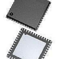
ASD5010L1000INT Arctic Silicon Devices, ASD5010L1000INT Datasheet - Page 33

ASD5010L1000INT
Manufacturer Part Number
ASD5010L1000INT
Description
ADC (A/D Converters) A-D Conv, Dig Gain Single 8 bit 1 GSPS
Manufacturer
Arctic Silicon Devices
Datasheet
1.ASD5010L500INT.pdf
(35 pages)
Specifications of ASD5010L1000INT
Number Of Converters
1
Number Of Adc Inputs
2
Conversion Rate
1000 MSPs
Resolution
8 bit
Snr
49.8 dB
Voltage Reference
1 V
Supply Voltage (max)
2 V
Supply Voltage (min)
1.7 V
Maximum Power Dissipation
710 mW
Maximum Operating Temperature
+ 85 C
Mounting Style
SMD/SMT
Package / Case
QFN-48
Input Voltage
1.8 V
Minimum Operating Temperature
- 40 C
Lead Free Status / RoHS Status
Lead free / RoHS Compliant
Preliminary Product Specification
all circuitry in the clock distribution. It is of utmost
importance to avoid crosstalk between the ADC output
bits and the clock and between the analog input signal
and the clock since such crosstalk often results in
harmonic distortion.
The jitter performance is improved with reduced rise and
fall times of the input clock. Hence, optimum jitter
performance is obtained with LVDS or LVPECL clock with
fast edges. CMOS and sine wave clock inputs will result
in slightly degraded jitter performance.
If the clock is generated by other circuitry, it should be re-
timed with a low jitter master clock as the last operation
before it is applied to the ADC clock input.
Application Usage Example
This section gives an overview on how ASD5010 can be
used in an application utilizing all active modes with a
single clock source. The example assumes that a 1GHz
clock source is applied. A differential clock should be
used, and can be generated from a single ended crystal
oscillator, using a transformer or balun in conjunction with
ac-coupling to convert from single ended to differential
signal.
Start-up Initialization
The start-up sequence will be as follows:
ASD5010
⁻ Apply power
⁻ Apply reset (RESETN low, then high, or SPI command
⁻ Set power down (PD pin high or SPI command 0x0F
⁻ Set LVDS bit clock phase (phase_ddr, register 0x42)) if
⁻ Select operating mode, for instance dual channel
⁻ Set active mode (PD pin low or SPI command 0x0F
⁻ Select analog inputs, for instance input 1 on channel 1
0x00 0x0001)
0x0200)
other than default must be used (depends on the
receiver).
mode, and clock divider factor (SPI command 0x31
0x0102).
0x0000)
and input 3 on channel 2 (SPI commands 0x3A 0202
and 0x3B 0808)
rev 2.0, 2010.11.08
Page 33 of 35
Change Mode
When changing operational mode, power down must be
activated due to internal synchronization routines. A
typical mode change will then be like this:
Table 26 gives an overview of the operational modes in
this example and the SPI commands to apply for each
mode.
Select Analog Input
When an operational mode is selected, the analog inputs
can be changed 'on-the-fly'. To change analog input one
merely have to apply the dedicated SPI commands. The
change will occur instantaneously at the end of each SPI
command.
Single channel
Dual channel
Quad channel
Single channel
Dual channel
Quad channel
⁻ Set power down (PD pin high or SPI command 0x0F
⁻ Change mode to for example Single channel mode
⁻ Set active mode (PD pin low or SPI command 0x0F
⁻ Select analog inputs, for instance Input 1 (SPI
0x0200)
(SPI command 0x31 0x0001)
0x0000)
commands 0x3A 0202 and 0x3B 0202)
Operating mode
Operating mode
Table 27: Example of some analog input selections
Table 26: Overview of operating modes and setup
Sampling
Signal input
Ch1: IP2/IN2
Ch2: IP3/IN3
Ch1: IP4/IN4
Ch2: IP3/IN3
Ch3: IP2/IN2
Ch4: IP1/IN1
[MSPS]
speed
selection
1000
500
250
conditions
IP4/IN4
divider
Clock
factor
1
2
4
0x3A 1010, 0x3B 1010
0x3A 0404, 0x3B 0808
0x3A 1008, 0x3B 0402
SPI commands
SPI command for
and clock divider
mode selection
0x31 0x0001
0x31 0x0102
0x31 0x0204
Confidential


