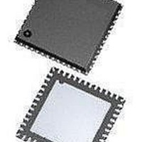
ASD5010L1000INT Arctic Silicon Devices, ASD5010L1000INT Datasheet - Page 12

ASD5010L1000INT
Manufacturer Part Number
ASD5010L1000INT
Description
ADC (A/D Converters) A-D Conv, Dig Gain Single 8 bit 1 GSPS
Manufacturer
Arctic Silicon Devices
Datasheet
1.ASD5010L500INT.pdf
(35 pages)
Specifications of ASD5010L1000INT
Number Of Converters
1
Number Of Adc Inputs
2
Conversion Rate
1000 MSPs
Resolution
8 bit
Snr
49.8 dB
Voltage Reference
1 V
Supply Voltage (max)
2 V
Supply Voltage (min)
1.7 V
Maximum Power Dissipation
710 mW
Maximum Operating Temperature
+ 85 C
Mounting Style
SMD/SMT
Package / Case
QFN-48
Input Voltage
1.8 V
Minimum Operating Temperature
- 40 C
Lead Free Status / RoHS Status
Lead free / RoHS Compliant
Preliminary Product Specification
Start up Initialization
As part of the ASD5010 power-on sequence both a reset and a power down cycle have to be applied to ensure correct
start-up initialization. Reset can be done in one of two ways:
Power down cycling can be done in one of two ways:
Serial Interface
The ASD5010 configuration registers can be accessed through a serial interface formed by the pins SDATA (serial
interface data), SCLK (serial interface clock) and CSN (chip select, active low). The following occurs when CSN is set
low:
Multiples of 24-bit words data can be loaded within a single active CSN pulse. If more than 24 bits are loaded into SDATA
during one active CSN pulse, only the first 24 bits are kept. The excess bits are ignored. Every 24-bit word is divided into
two parts:
Acceptable SCLK frequencies are from 20MHz down to a few hertz. Duty-cycle does not have to be tightly controlled.
Timing Diagram
Figure 4 shows the timing of the serial port interface. Table 4 explains the timing variables used in figure 4.
ASD5010
SDATA
SCLK
CSN
1.
2.
1.
2.
●
●
●
●
●
By applying a low-going pulse (minimum 20 ns) on the RESETN pin (asynchronous).
By using the serial interface to set the 'rst' bit high. Internal registers are reset to default values when this bit is
set. The 'rst' bit is self-reset to zero. When using this method, do not apply any low-going pulse on the RESETN
pin.
By applying a high-going pulse (minimum 20 ns) on the PD pin (asynchronous).
By cycling the 'pd' bit in register 0F
Serial data are shifted into the chip
At every rising edge of SCLK, the value present at SDATA is latched
SDATA is loaded into the register every 24th rising edge of SCLK
The first eight bits form the register address
The remaining 16 bits form the register data
A7
t
t
t
t
t
t
t
t
A6
cs
ch
hi
lo
ck
s
h
cs
Parameter
A5
A4
A3
Setup time between CSN and SCLK
Hold time between CSN and SCLK
SCLK high time
SCLK low time
SCLK period
Data setup time
Data hold time
t
A2
hi
t
lo
Table 4: Serial Port Interface timing definitions
A1
A0
Figure 4: Serial Port Interface timing
hex
D15 D14 D13 D12 D11 D10 D9
to high (reg value '0200'
t
ck
Description
rev 2.0, 2010.11.08
Page 12 of 35
t
s
t
h
hex
) and then low (reg value '0000'
D8
D7
D6
8
8
20
20
50
5
5
D5
Minimum
value
D4
D3 D2
ns
ns
ns
ns
ns
ns
ns
Unit
t
D1
ch
hex)
D0
.
Confidential
t
chi


